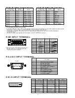
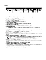

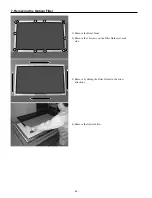


V
S
AND V
d
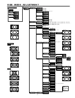
ADJUSTMENT
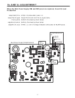
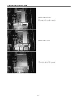
When the Main Power Supply PCB and PDP panel are replaced, Vs and Vd must
be adjusted.
Adjustment time Within 3 minutes after power on.
Adjustment signal Adjust the Vs and Vd in the no-signal state.
Check points Refer to the drawing shown below.
Adjustment points Refer to the drawing shown below.
Adjustment value /- 0.1V of voltage indicated on the label on the PDP panel.
Vs & Vd check point
P6
T4
T3
T2
L4
L2
L1
P5
P6
C56
RV3
Vs ADJ.
RV4
Vd ADJ.
1
9
1 pin Vs
2 pin Vs
4 pin Vd
5 pin GND
6 pin GND
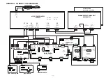
Main Power Supply PCB (PFW-423)
- 17 -
Содержание PDS4233W/E-H
Страница 1: ...PDS4233W E H PDS4234W E S Copy Prohibited FUJITSU GENERAL Proprietar y ...
Страница 35: ... 34 MEMO ...
Страница 36: ...January 2002 Printed in Japan 0202J1957 ...