


Page 7 of 28
Rev. A
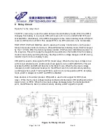
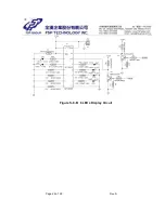
3 Control pow er circuit
The control power (+ 12Vdc and + 5Vdc) comes from the following sources (Figure S-2).
3.1
Start w ithout input AC pow er ( Cold start) :
A “Cold start “is described as follows:
3.1.1
When “ON/ OFF” switch (SW1) is pressed, a positive battery current flows
through SW1 to charge C15.
3.1.2
Q12 base receives a HI pulse and turns on (signal bypass C15 at t= 0, and
charge C15 at t> 0).
3.1.3
When Q12 turns on, the Q12 collector will drop to LOW and turn on Q11
(MPS2907A).
3.1.4
When Q11 turns on, the positive battery voltage via Q12 collector and
establishes a + 12Vdc power supply. The + 12Vdc power supply passes
through U03 (78L05) generating a + 5Vdc logic power supply. And CPU
send HI signal (shutdown) to sustain Q12 on.
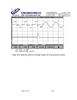
3.1.5
Figure W-1 shows the pulse on the C15, i.e. the base signal of Q12 during
the cold start.
3.2
Start w ith input AC pow er ( AC start) :
3.2.1
When we connect UPS to the utility, half-wave rectifier will activate Q12
through D2, ZD1, and Q16.
3.2.2
If “ON/ OFF” switch is pressed, Q11 turns on and establishes a + 12Vdc and
+ 5Vdc power supply similar to “Cold start”.
The SHUTDOWN network, triggered by pin 15 of the CPU, is used to shutdown the UPS on
battery mode. When a battery is in low battery voltage status, the CPU sends a “Low”
signal to turn off Q12. This causes Q11 to be turned off and isolates the control
power from batteries.
Содержание 1500 Series
Страница 2: ...Page 1 of 28 Rev A UNINTERRUPTIBLE POWER SYSTEM SPECIFICATION EP 1000 1500 2000 Series ...
Страница 3: ...Page 2 of 28 Rev A 1 0 Revision Summary REVI SI ON SECTI ON DESCRI PTI ON Rev A Formal Release ...
Страница 9: ...Page 8 of 28 Rev A Figure S 2 Control Power Circuit CH1 C15 å GND Figure W 1 Cold Start ...
Страница 11: ...Page 10 of 28 Rev A Figure S 3 B Charger Control Circuit ...
Страница 16: ...Page 15 of 28 Rev A CH1 DS N CH2 Output Voltage 1 200V Figure W 3 Control logic 1 ...
Страница 19: ...Page 18 of 28 Rev A Figure S 6 CPU Control Circuit ...
Страница 23: ...Page 22 of 28 Rev A Figure S 8 B 6 LEDs Display Circuit ...
Страница 28: ...Page 27 of 28 Rev A Figure W 7 Battery Mode Examination Flowchart ...
Страница 29: ...Page 28 of 28 Rev A Figure W 8 Line Mode Examination Flowchart ...


