


Sensors
18
Freescale Semiconductor
MMA7455L
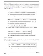
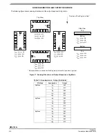
SPI Slave Interface
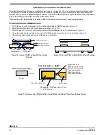
The MMA7455L also uses serial peripheral interface communication as a digital communication. The SPI communication is pri-
marily used for synchronous serial communication between a master device and one or more slave devices. See
for
an example of how to configure one master with one MMA745xL device. The MMA7455L is always operated as a slave device.
Typically, the master device would be a microcontroller which would drive the clock (SPC) and chip select (CS) signals.
The SPI interface consists of two control lines and two data lines: CS, SPC, SDI, and SDO. The CS, also known as Chip Select,
is the slave device enable which is controlled by the SPI master. CS is driven low at the start of a transmission. CS is then driven
high at the end of a transmission. SPC is the Serial Port Clock which is also controlled by the SPI master. SDI and SDO are the
Serial Port Data Input and the Serial Port Data Output. The SDI and SDO data lines are driven at the falling edge of the SPC and
should be captured at the rising edge of the SPC.
Read and write register commands are completed in 16 clock pulses or in multiples of 8, in the case of a multiple byte read/write.
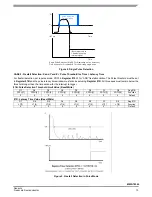
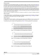
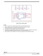
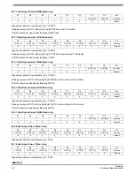
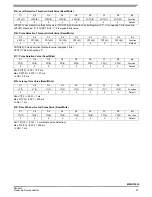
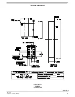
SPI Read Operation
A SPI read transfer consists of a 1-bit Read/Write signal, a 6-bit address, and 1-bit don’t care bit. (1-bit R/W=0 + 6-bits address
+ 1-bit don’t care). The data to read is sent by the SPI interface during the next transfer. See
and
for the
timing diagram for an 8-bit read in 4 wire and 3 wire modes, respectively.
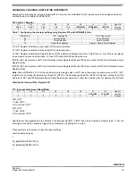
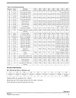
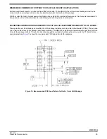
SPI Write Operation
In order to write to one of the 8-bit registers, an 8-bit write command must be sent to the MMA7455L. The write command consists
of an MSB (0=read, 1=write) to indicate writing to the MMA7455L register, followed by a 6-bit address and 1 don’t care bit.
The command should then be followed the 8-bit data transfer. See
for the timing diagram for an 8-bit data write.
Figure 11. SPI Timing Diagram for 8-Bit Register Read (4 Wire Mode)
Figure 12. SPI Timing Diagram for 8-Bit Register Read (3 Wire Mode)
Figure 13. SPI Timing Diagram for 8-Bit Register Write (3 Wire Mode)