


Device User Guide — 9S12DT128DGV2/D V02.16
71
Freescale Semiconductor
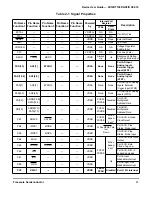
2.3.43 PP5 / KWP5 / PWM5 — Port P I/O Pin 5
PP5 is a general purpose input or output pin. It can be configured to generate an interrupt causing the MCU
to exit STOP or WAIT mode. It can be configured as Pulse Width Modulator (PWM) channel 5 output.
2.3.44 PP4 / KWP4 / PWM4 — Port P I/O Pin 4
PP4 is a general purpose input or output pin. It can be configured to generate an interrupt causing the MCU
to exit STOP or WAIT mode. It can be configured as Pulse Width Modulator (PWM) channel 4 output.
2.3.45 PP3 / KWP3 / PWM3 / SS1 — Port P I/O Pin 3
PP3 is a general purpose input or output pin. It can be configured to generate an interrupt causing the MCU
to exit STOP or WAIT mode. It can be configured as Pulse Width Modulator (PWM) channel 3 output. It
can be configured as slave select pin SS of the Serial Peripheral Interface 1 (SPI1).
2.3.46 PP2 / KWP2 / PWM2 / SCK1 — Port P I/O Pin 2
PP2 is a general purpose input or output pin. It can be configured to generate an interrupt causing the MCU
to exit STOP or WAIT mode. It can be configured as Pulse Width Modulator (PWM) channel 2 output. It
can be configured as serial clock pin SCK of the Serial Peripheral Interface 1 (SPI1).
2.3.47 PP1 / KWP1 / PWM1 / MOSI1 — Port P I/O Pin 1
PP1 is a general purpose input or output pin. It can be configured to generate an interrupt causing the MCU
to exit STOP or WAIT mode. It can be configured as Pulse Width Modulator (PWM) channel 1 output. It
can be configured as master output (during master mode) or slave input pin (during slave mode) MOSI of
the Serial Peripheral Interface 1 (SPI1).
2.3.48 PP0 / KWP0 / PWM0 / MISO1 — Port P I/O Pin 0
PP0 is a general purpose input or output pin. It can be configured to generate an interrupt causing the MCU
to exit STOP or WAIT mode. It can be configured as Pulse Width Modulator (PWM) channel 0 output. It
can be configured as master input (during master mode) or slave output (during slave mode) pin MISO of
the Serial Peripheral Interface 1 (SPI1).
2.3.49 PS7 / SS0 — Port S I/O Pin 7
PS7 is a general purpose input or output pin. It can be configured as the slave select pin SS of the Serial
Peripheral Interface 0 (SPI0).
2.3.50 PS6 / SCK0 — Port S I/O Pin 6
PS6 is a general purpose input or output pin. It can be configured as the serial clock pin SCK of the Serial
Peripheral Interface 0 (SPI0).
Содержание MC9S12A128
Страница 6: ...Device User Guide 9S12DT128DGV2 D V02 16 6 Freescale Semiconductor...
Страница 18: ...Device User Guide 9S12DT128DGV2 D V02 16 18 Freescale Semiconductor...
Страница 24: ...Device User Guide 9S12DT128DGV2 D V02 16 24 Freescale Semiconductor...
Страница 56: ...Device User Guide 9S12DT128DGV2 D V02 16 56 Freescale Semiconductor...
Страница 76: ...Device User Guide 9S12DT128DGV2 D V02 16 76 Freescale Semiconductor...
Страница 80: ...Device User Guide 9S12DT128DGV2 D V02 16 80 Freescale Semiconductor...
Страница 84: ...Device User Guide 9S12DT128DGV2 D V02 16 84 Freescale Semiconductor...
Страница 95: ...Device User Guide 9S12DT128DGV2 D V02 16 95 Freescale Semiconductor...
Страница 96: ...Device User Guide 9S12DT128DGV2 D V02 16 96 Freescale Semiconductor...
Страница 116: ...Device User Guide 9S12DT128DGV2 D V02 16 116 Freescale Semiconductor...
Страница 118: ...Device User Guide 9S12DT128DGV2 D V02 16 118 Freescale Semiconductor...
Страница 126: ...Device User Guide 9S12DT128DGV2 D V02 16 126 Freescale Semiconductor...
Страница 128: ...Device User Guide 9S12DT128DGV2 D V02 16 128 Freescale Semiconductor...
Страница 140: ...Device User Guide 9S12DT128DGV2 D V02 16 140 Freescale Semiconductor...
Страница 141: ...Device User Guide 9S12DT128DGV2 D V02 16 141 Freescale Semiconductor User Guide End Sheet...


