


Device User Guide — 9S12DT128DGV2/D V02.16
107
Freescale Semiconductor
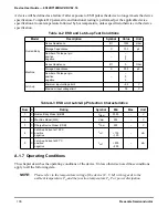
A.2 ATD Characteristics
This section describes the characteristics of the analog to digital converter.
A.2.1 ATD Operating Characteristics
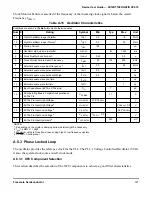
The
shows conditions under which the ATD operates.
The following constraints exist to obtain full-scale, full range results:
V
SSA
≤
V
RL
≤
V
IN
≤
V
RH
≤
V
DDA
.
This constraint exists since the sample buffer amplifier can not drive
beyond the power supply levels that it ties to. If the input level goes outside of this range it will effectively
be clipped.
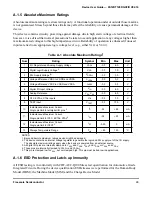
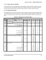
Table A-8 ATD Operating Characteristics
A.2.2 Factors influencing accuracy
Three factors – source resistance, source capacitance and current injection – have an influence on the
accuracy of the ATD.
A.2.2.1 Source Resistance:
Due to the input pin leakage current as specified in
in conjunction with the source resistance
there will be a voltage drop from the signal source to the ATD input. The maximum source resistance R
S
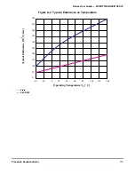
Conditions are shown in (Table A-4) unless otherwise noted
Num C
Rating
Symbol
Min
Typ
Max
Unit
1
D
Reference Potential
Low
High
V
RL
V
RH
V
SSA
V
DDA
/2
V
DDA
/2
V
DDA
V
V
2
C Differential Reference Voltage
1
NOTES
:
1. Full accuracy is not guaranteed when differential voltage is less than 4.50V
V
RH
-V
RL
4.50
5.00
5.25
V
3
D ATD Clock Frequency
f
ATDCLK
0.5
2.0
MHz
4
D
ATD 10-Bit Conversion Period
Clock Cycles
2
Conv, Time at 2.0MHz ATD Clock f
ATDCLK
2. The minimum time assumes a final sample period of 2 ATD clocks cycles while the maximum time assumes a final sample
period of 16 ATD clocks.
N
CONV10
T
CONV10
14
7
28
14
Cycles
µ
s
5
D
ATD 8-Bit Conversion Period
Conv, Time at 2.0MHz ATD Clock f
ATDCLK
N
CONV8
T
CONV8
12
6
26
13
Cycles
µ
s
6
D Stop Recovery Time (V
DDA
=5.0 Volts)
t
SR
20
µ
s
7
P Reference Supply current (Both ATD modules on)
I
REF
0.75
mA
8
P Reference Supply current (Only one ATD module on)
I
REF
0.375
mA
Содержание MC9S12A128
Страница 6: ...Device User Guide 9S12DT128DGV2 D V02 16 6 Freescale Semiconductor...
Страница 18: ...Device User Guide 9S12DT128DGV2 D V02 16 18 Freescale Semiconductor...
Страница 24: ...Device User Guide 9S12DT128DGV2 D V02 16 24 Freescale Semiconductor...
Страница 56: ...Device User Guide 9S12DT128DGV2 D V02 16 56 Freescale Semiconductor...
Страница 76: ...Device User Guide 9S12DT128DGV2 D V02 16 76 Freescale Semiconductor...
Страница 80: ...Device User Guide 9S12DT128DGV2 D V02 16 80 Freescale Semiconductor...
Страница 84: ...Device User Guide 9S12DT128DGV2 D V02 16 84 Freescale Semiconductor...
Страница 95: ...Device User Guide 9S12DT128DGV2 D V02 16 95 Freescale Semiconductor...
Страница 96: ...Device User Guide 9S12DT128DGV2 D V02 16 96 Freescale Semiconductor...
Страница 116: ...Device User Guide 9S12DT128DGV2 D V02 16 116 Freescale Semiconductor...
Страница 118: ...Device User Guide 9S12DT128DGV2 D V02 16 118 Freescale Semiconductor...
Страница 126: ...Device User Guide 9S12DT128DGV2 D V02 16 126 Freescale Semiconductor...
Страница 128: ...Device User Guide 9S12DT128DGV2 D V02 16 128 Freescale Semiconductor...
Страница 140: ...Device User Guide 9S12DT128DGV2 D V02 16 140 Freescale Semiconductor...
Страница 141: ...Device User Guide 9S12DT128DGV2 D V02 16 141 Freescale Semiconductor User Guide End Sheet...


