


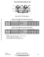


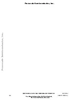


ELECTRICAL CHARACTERISTICS
MC68332
A-26
USER’S MANUAL
Notes:
1. All AC timing is shown with respect to 20% V
DD
and 70% V
DD
levels unless otherwise noted.
2. In formula, n = External SCK rise + External SCK fall time
3. Data can be recognized properly with longer transition times as long as MOSI/MISO signals from external sourc-
es are at valid V
OH
/V
OL
prior to SCK transitioning between valid V
OL
and V
OH
. Due to process variation, logic
decision point voltages of the data and clock signals can differ, which can corrupt data if slower transition times
are used.
Table A-9 QSPI Timing
(V
DD
= 5.0 Vdc
±
10%, V
SS
= 0 Vdc, T
A
= T
L
to T
H,
200 pF load on all QSPI pins)
Num
Function
Symbol
Min
Max
Unit
Operating Frequency
Master
Slave
f
op
DC
DC
1/4
1/4
System Clock Frequency
System Clock Frequency
1
Cycle Time
Master
Slave
t
qcyc
4
4
510
—
t
cyc
t
cyc
2
Enable Lead Time
Master
Slave
t
lead
2
2
128
—
t
cyc
t
cyc
3
Enable Lag Time
Master
Slave
t
lag
—
2
1/2
—
SCK
t
cyc
4
Clock (SCK) High or Low Time
Master
Slave
2
t
sw
2 t
cyc
– 60
2 t
cyc
– n
255 t
cyc
—
ns
ns
5
Sequential Transfer Delay
Master
Slave (Does Not Require Deselect)
t
td
17
13
8192
—
t
cyc
t
cyc
6
Data Setup Time (Inputs)
Master
Slave
t
su
30
20
—
—
ns
ns
7
Data Hold Time (Inputs)
Master
Slave
t
hi
0
20
—
—
ns
ns
8
Slave Access Time
t
a
—
1
t
cyc
9
Slave MISO Disable Time
t
dis
—
2
t
cyc
10
Data Valid (after SCK Edge)
Master
Slave
t
v
—
—
50
50
ns
ns
11
Data Hold Time (Outputs)
Master
Slave
t
ho
0
0
—
—
ns
ns
12
Rise Time
Input
3
Output
t
ri
t
ro
—
—
2
30
µ
s
ns
13
Fall Time
Input
3
Output
t
fi
t
fo
—
—
2
30
µ
s
ns
F
re
e
sc
a
le
S
e
m
ic
o
n
d
u
c
to
r,
I
Freescale Semiconductor, Inc.
For More Information On This Product,
Go to: www.freescale.com
n
c
.
..