


12
13
Pin Assignm.
Function
Internal wiring
Description
17
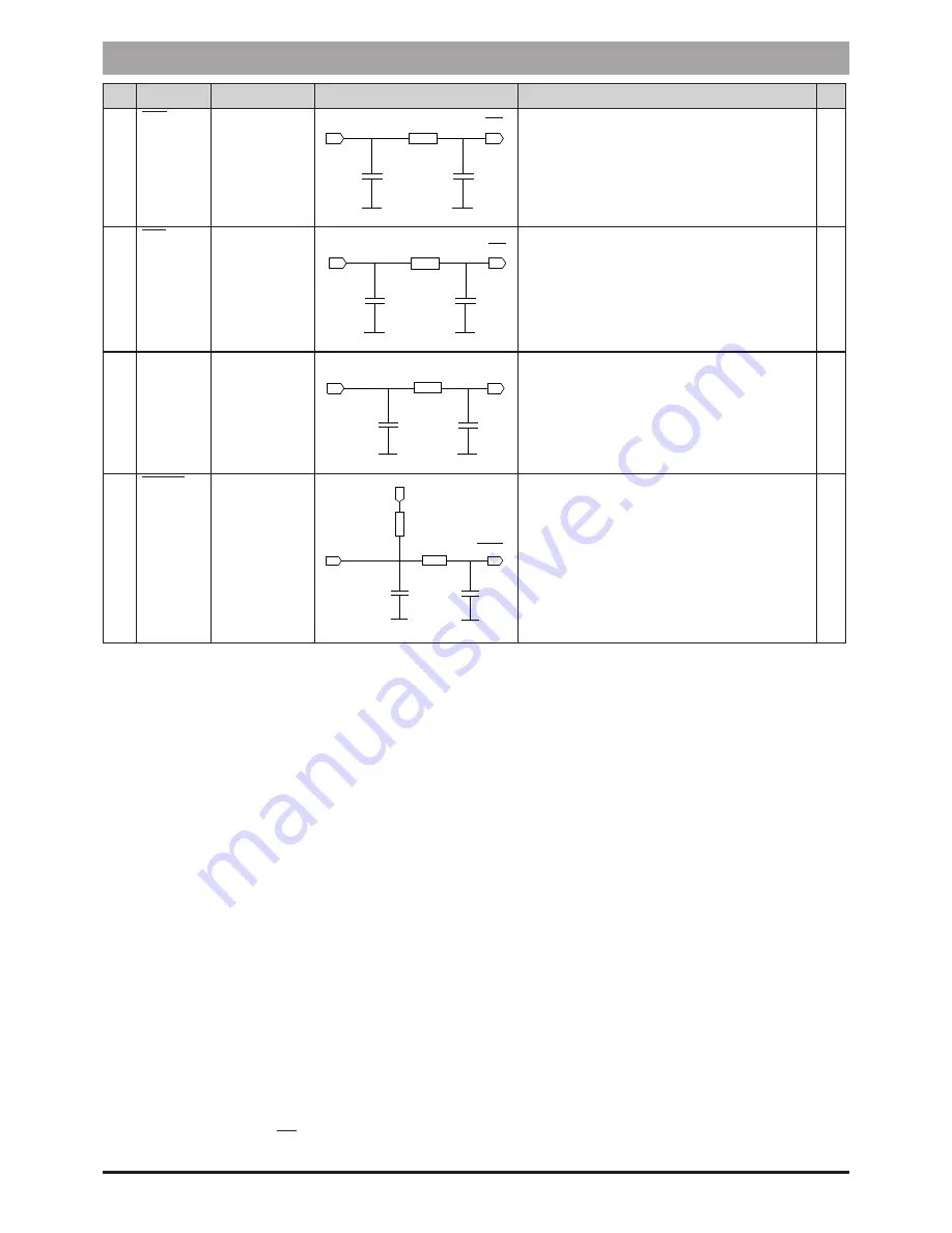
RXC
Output, digital
RXC
100R
1n
1n
Rec er
eiv
Receive timing / clock
4)
5)
18
UET
Output, digital
UET
220R
1n
1n
Ov r
e -temperature
r
cont ol
Status output over-temperature
If the temperature of the power amplifier exceeds ap-
prox. 80 °C, the output will have LOW level.
4)
11)
19
RS232_
OUT
Output, digital,
RS232
220R
RS232_OUT
15
0p
15
0p
Opt on to m r oproc so
i al
i c
es r
o 232 t
sc v r
or t RS
ran ei e
Data output to the serial interface of the PC
Pin 2 (RXD) with 9 pin interface;
Pin 3 (RXD) with 25 pin interface.
2)
4)
20
ERROR
Output, digital
1n
1n
1K
+
5V
220R
ERROR
R
MICROPROCESSO
This output has LOW level for approx. 1.3 s in case of
faulty actions.
Idle condition: HIGH
Signal level: LOW for approx. 1.3 s
3)
4)
1) The input can be set to active LOW or active HIGH via the setting of the parameters; the PTT is set to active LOW by de-
fault.
2) Optionally available with similar to TTL (4,0 ... 5,0 V).
3) The duration of the display can be programmed via software.
4) The internal wiring additionally serves as EMV protection against radiation or emission.
5) The RXC (Clock) is only made available in receiving operation at the user interface at devices with FFSK modulator.
6) The data that is to be send has to be synchronous to the generated clock TXC at the version synchronous.
7) A synchronization of the data takes automatically place in the device at the version asynchronous. In this connection, the
norm V.24/V.28 (1 start bit, 8 data bit, no parity, 1 stop bit, asynchronous) is to be kept at the data input. Since an additional
loss of data is caused during sending at this version, the RTS signal after the last transferred data bit has to remain acti-
vated correspondingly longer (see chapter
11. Timing charts of the unit
).
8) Two binary zeros and two binary ones (33 h, 66 h, 99 h oder cc h) have to be transmitted alternating to the synchronization
at devices with GMSK modulator. A change between a binary zero and a binary one (55h, AAh) should be avoided. This
sequence brings the quickest synchronization, but it can possibly lead to a higher fault rate at the data transmission.
The synchronization sequence has to have a length of at least 16 bit.
After the synchronization, you should send a start bit in order to mark the beginning of the data transmission for the opposite
station. A stop bit should be at the end of the useful data so that the opposite station recognizes the end of the transmission.
9) ASCII data or a scrambler, so that bit changes for binary data are ensured, are to be used at devices with GMSK modulator.
10) The data can be evaluated after receipt of the synchronization sequence
.
11) 100mW versions: output
UET
is not effective
General instructions
Содержание WZ FSE 2-2
Страница 1: ...WZ FSE 2 2 Instructions for use...