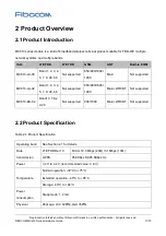

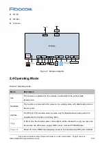


Reproduction forbidden without Fibocom Wireless Inc. written authorization - All rights reserved.
FIBOCOM MC610 Series Hardware Guide
20/70
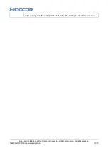
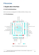
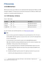
Pin Pin Name
I/O
Voltage
Domain
Reset
Value
Description
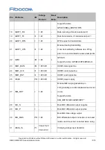
67
ISENSE
I
-
-
Charging current detection signal
68
GND
G
-
-
Ground
69
LCD_CS
O
1.8V
-
LCD chip selection signal
Multiplexing function LCD_CS/GPIO3
70
GND
G
-
-
Ground
71
USB_BOOT/KEY_IN0 I
1.8V
-
Key pad input 0
USB_BOOT rise to be in the DL mode
KEYIN cannot be used as a key alone.
72
VBAT_SENSE
I
Vmax=4.2V
Vmin=3.4V
Vnorm=3.8V
-
The battery voltage detection signal should
be close to the anode of the battery terminal
as far as possible. If the charging function is
not used, it should be connected to VBAT.
73
VDRV
O
-
-
Charging drive control voltage of external
PMOS
74
LCD_RSTB
O
1.8V/3V*
-
LCD_RST
This pin does not support GPIO function.
75
KEY_OUT1
O
1.8V
-
KEYOUT1
KEYOUT cannot be used alone.
Multiplexing function KEY_OUT1/U2CTS
76
KEY_OUT2
O
1.8V
-
KEYOUT2
KEYOUT cannot be used alone.
Multiplexing function KEY_OUT2/U2RTS
77
U3RXD
I
1.8V/3V*
-
Data receiving of module serial port 3
Multiplexing function
SD1_D2/GPIO27/U2CTS/U3RXD/SPI2DIO_0
78
U3TXD
O
1.8V/3V*
-
Data transmission of module serial port 3
Multiplexing function


