


Reproduction forbidden without Fibocom Wireless Inc. written authorization - All Rights Reserved.
FM350-GL Hardware Guide
Page 20 of 59
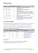
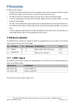
Parameters
Minimum
Typical
Maximum
Unit
3.3V logic level
3.135
3.3
3.465
V
V
IH
2.3
3.3
3.465
V
V
IL
-0.3
0
0.3
V
3.3
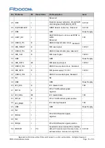
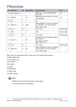
Control Signal
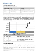
The FM350 module provides two control signals for power on/off and reset operations, the pin defined as
shown in the following table:
Pin
Pin Name
I/O
Reset Value
Functions
Level
6
FULL_CARD_POWER
_OFF#
I
PU
Module power on/off input,
internal pull up(35
0KΩ)
Power on: High/Floating
Power off: Low
3.3/1.8V
67
RESET#
I
PU
WWAN reset input, active low,
internal pull up(350
KΩ)
1.8V
50
PERST#
I
PU
Asserted to reset module PCIe
interface default. If module went into
core dump, it will reset whole
module, not only PCIe interface.
Active low,
internal pull up(10KΩ)
3.3/1.8V
Note
:
RESET# and PERST# need to be controlled by independent GPIO, and not shared with other
devices on the host.
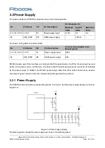
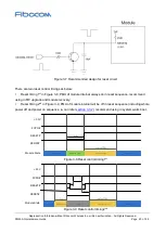
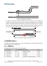
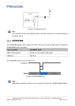
Module Start-Up
3.3.1.1
Start-up Circuit
The FCPO#( FULL_CARD_POWER_OFF #) pin needs an external 3.3V or 1.8V pull up for booting up.
AP (Application Processor) controls the module start-up. The recommended design is using a default PD
port to control FCPO#. It also should reserve a 100K pull down resistor on AP side. The circuit design is
shown in Figure 3-4:


