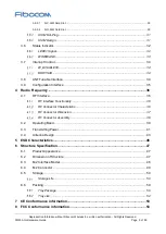


Reproduction forbidden without Fibocom Wireless Inc. written authorization - All Rights Reserved.
FM350-GL Hardware Guide
Page 15 of 59
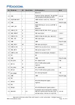
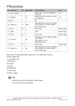
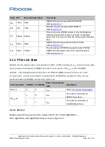
Pin Pin Name
I/O
Reset Value
Pin Description
Level
Reserved
25 DPR
I
Dynamic power reduction - Body SAR
control signal (SAR_BACK_OFF)
3.3/1.8V
26 W_DISABLE2#
I
GNSS disable, active low,
Reserved
3.3/1.8V
27 GND
-
-
GND
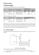
Power Supply
28 UART_RX
I
UART RXD input, can mux as DPR2 or
GPIO.
Reserved
1.8V
29
USB3.0_TX-
O
-
USB3.0 transmit data minus,
reserved
-
30 UIM_RESET
O
SIM reset signal
1.8V/3V
31
USB3.0_TX+
O
-
USB3.0 transmit data plus,
reserved
-
32 UIM_CLK
O
SIM clock Signal
1.8V/3V
33 GND
-
-
GND
Power Supply
34 UIM_DATA
I/O
SIM data input/output
1.8V/3V
35
USB3.0_RX-
I
-
USB3.0 receive data minus,
reserved
-
36 UIM_PWR
O
-
SIM power supply, 1.8V/3V
1.8V/3V
37
USB3.0_RX+
I
-
USB3.0 receive data plus,
reserved
-
38 NC
-
NC
-
39 GND
-
-
GND
Power Supply
40
I2C_SCL
O
-
I2C master clock
1.8V
41 PETn0
O
-
PCIe TX differential signals
negative
-
42
I2C_SDA
I/O
I2C master data
1.8V
43 PETp0
O
-
PCIe TX differential signals positive
-
44
I2C_IRQ#
I
-
I2C interrupt request
1.8V
45 GND
-
-
GND
Power Supply
46
NC
-
-
-
-
47 PERn0
I
-
PCIe RX differential signals
negative
-
48
NC
-
-
-
-
49 PERp0
I
-
PCIe RX differential signals positive
-
50 PERST#
I
PU
Asserted to reset module PCIe interface
default. If module went into core dump, it
will reset whole module, not only PCIe
3.3/1.8V