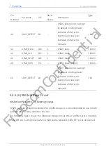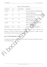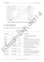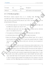
Pin Name
I/O
Pin
Number
Description
REFCLKP
PCIE_CLK_P
55
PCIE reference clock signal positive
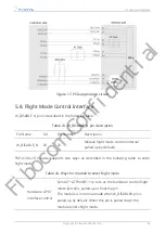
5.7.1. PCIe Routing Rules
FM101-NA-20 module supports PCIe 2.0 x1, including three differential pairs:
transmitting pair TXP/N, receiving pair RXP/N and clock pair CLKP/N.
PCIe can achieve the maximum transmission rate of 5GT/s. The following rules must be
strictly followed in PCB layout:
•
The differential signal pairs are required to be parallel traces with equal length, and
the difference in length is less than 0.15 mm.
•
The differential signal pair traces shall be as short as possible and be controlled
within 15 inch (380 mm) for AP end.
•
The impedance of differential signal pair traces is controlled to be 100Ω±10%.
•
Avoid discontinuous reference ground, such as segment and space.
•
When the differential signal traces go through different layers, the via hole of
ground signal should be close to that of signal, and generally, each pair of signals
require 1-3 ground signal via holes and the traces shall never cross the segment of
plane.
•
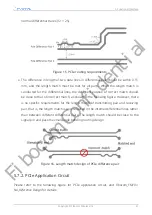
Try to avoid bended traces and avoid introducing common-mode noise in the
system, which will influence the signal integrity and EMI of differential pairs. As
shown in the following Figure, the bending angle of all traces should be equal to or
greater than 135°, the spacing between differential pair traces should be larger
than 20mil, and the traces caused by bending should be greater than 1.5 times
trace width at least. When a serpentine route is used for length match with another
route, the bended length of each segment shall be at least 3 times the route width
(
≥
3W). The largest spacing between the bended part of the serpentine trace and
another one of the differential traces must be less than 2 times the spacing of
5. Functional Interface
Copyright © Fibocom Wireless Inc.
40
Fibocom Confidential

