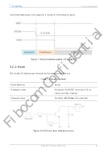
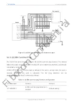
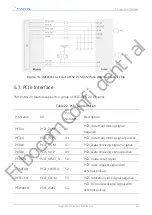
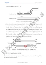
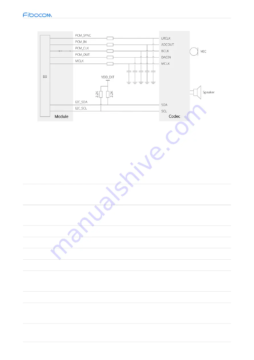
Figure 14. Reference circuit of the PCM interface external Codec chip
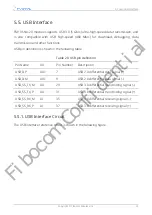
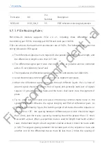
5.7. PCIe Interface
FM101-NA-20 module supports a group of PCIE GEN 2.0 x 1 lanes.
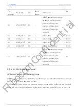
Table 22. PCIe pin definition
Pin Name
I/O
Pin
Number
Description
PETn0
PCIE_TX_M
41
PCIE_data transmitting signal
negative
PETp0
PCIE_TX_P
43
PCIE_data transmitting signal positive
PERn0
PCIE_RX_M
47
PCIE_Data receiving signal negative
PERp0
PCIE_RX_P
49
PCIE_Data receiving signal positive
PERST#
PCIE_RESET_N
50
PCIE mode reset signal
CLKREQ#
PCIE_CLKREQ
52
PCIE clock request signal with
external pull-up
REFCLKN
PCIE_CLK_M
53
PCIE reference clock signal negative
PEWAKE#
PCIE_WAKE
54
PCIE RC mode wake-up signal with
external pull-up
5. Functional Interface
Copyright © Fibocom Wireless Inc.
39
Fibocom Confidential


