background image

2007-11-19 

Page 21 of 35 

IT321_Tech_doc_12 


4.6.1  Active GPS antenna 

The customer may use an external active GPS antenna for e.g. in 
mobile or indoor usage. It is suggested the active antenna has a net 
gain 

including cable loss

 in the range from +10 dB to +25 dB. 

NOTE 

Max antenna bias current is 15mA. Antenna 
bias circuit has internal short circuit protec-
tion. At short circuit condition the antenna 
bias current is limited to abt. 60mA and the 
navigation data output will be stopped. Navi-
gation will recover automatically when short 
circuit is removed. 


4.7 UART 

The device supports UART communication via one serial port A.  

The default configuration for baud rates and respective protocols can 
be changed by commands via NMEA or SiRF binary protocols 

(ref II & 

III)

. Any custom configuration stays active as long as supply VDD is 

active. 

I/O levels form the serial port is CMOS 1.8V compatible, not RS232 
compatible. Use an external level converter to provide CMOS 3.3V or 
RS232 levels when needed.  The RXA input can be left unconnected 
when not needed since it has internal pull up resistor. 

4.8 PPS 

The pulse-per-second (PPS) output provides a pulse signal for timing 
purposes. Pulse length (high state) is about 1us synchronized to full 
UTC second. I/O level is CMOS 1.8V compatible. 

4.9 ELCK 

The ECLK is available optionally for external clock input with special 
ROM version for A-GPS frequency aiding. Pull down (e.g. 10kohm) if 
not used. I/O level is CMOS 1.8V compatible. 

Содержание IT321

Страница 1: ...EV 1 2 TECHNICAL DESCRIPTION Fastrax IT321 OEM GPS Receiver This document describes the electrical connectivity and main functionality of the Fastrax IT321 OEM GPS Receiver November 19 2007 Fastrax Lt...

Страница 2: ...RKS Fastrax is trademark of Fastrax Ltd SiRF SiRFStar TM TricklePowerTM Push to FixTM SiRFDriveTM are registered trademark and trademarks of SiRF Technology Inc All other trademarks are trademarks or...

Страница 3: ...s max power dissipation 300mW oper temp range 30C 85C GPIO6 13 added to HW rev B added VDD ripple specification added ON_OFF tim ing removed solder profile picture added tape and reel spec changed App...

Страница 4: ...3 5 Procedure for re programming the flash firmware 14 4 CONNECTIVITY 16 4 1 Connection assignments 16 4 2 Power supply 18 4 3 Configuration select GPIO 6 2 18 4 4 Boot Control inputs 18 4 5 ON_OFF co...

Страница 5: ...6 2 PCB layout issues 27 7 IT321 APPLICATION BOARD 29 7 1 Card Terminal I O connector 29 7 2 Bill of materials PCB rev C 31 7 3 Circuit drawing rev C 32 7 4 Assembly drawing Top side rev C 33 7 5 Artw...

Страница 6: ...fastrax fi Ref File name Document name The following SiRF reference documents are also complementary reading for this document All operating and firmware related documentation is available from SiRF...

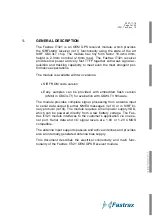
Страница 7: ...mples can be provided with embedded flash version 4Mbit in GSC3LTf for evaluation with GSWLT3 firmware The module provides complete signal processing from antenna input to serial data output in either...

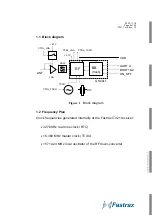
Страница 8: ...V CTRL_LNA ANT UART A BOOT1 2 VDD 2 7V CTRL_TCXO CTRL_TCXO CTRL_LNA ON_OFF Figure 1 Block diagram 1 2 Frequency Plan Clock frequencies generated internally at the Fastrax IT321 receiver 32768 Hz real...

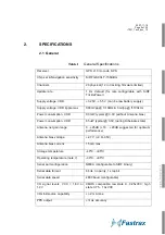
Страница 9: ...consumption VDD 90 mW typical 3 3V without Antenna bias Power consumption VDD 65 uW typical 3 3V during Hibernate state Antenna net gain range 0 25dB 10 20dB suggested for optimum performance Antenna...

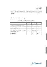
Страница 10: ...to First Fix and other GPS performance may be de graded 2 2 Absolute maximum ratings Table 2 Absolute maximum ratings Item Min Max unit Operating and storage temperature 40 85 C Power dissipation 300...

Страница 11: ...ation on GPS time satellite ephemeris and Last Known Good LKG position information provided by the non volatile back up block RTC RAM The power consumption will vary depending on the amount of satelli...

Страница 12: ...SBAS Disabled Enabled Enabled Static naviga tion filter Disabled Disabled Enabled Track smooth ing filter Enabled Enabled Enabled Internal DR Disabled Disabled Enabled Extended Ephemeris Disabled Ena...

Страница 13: ...main supply input VDD is kept active all the time even during Hibernate mode The Hibernate mode is entered by host interrupt at ON_OFF control input pulse low high low 62us Other internal blocks like...

Страница 14: ...ROM Normal mode Default 1 0 3 5 Procedure for re programming the flash firmware 1 Connect UART RXA and TXA signals to PC via RS232 converter 2 Set the module to UART boot mode Power up the module to...

Страница 15: ...2007 11 19 Page 15 of 35 IT321_Tech_doc_12 Figure 2 SiRFFlash utility settings...

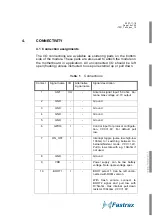
Страница 16: ...iption 1 ANT I O Antenna signal input 50 ohm An tenna bias voltage 2 7V output 2 GND Ground 3 GND Ground 4 GND Ground 5 GND Ground 6 GPIO6 I Control input for protocol configura tion VCC 1 8V For defa...

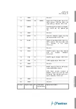
Страница 17: ...on for external clock input in A GPS version Pull low state with e g 10kohm if not used VCC 1 8V 17 GND Ground 18 RXA I UART A async Input Has internal pull up resistor 100kohm VCC 1 8V 19 TXA O UART...

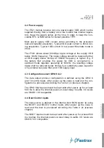
Страница 18: ...itched mode regulator operating at 100kHz the resulting voltage ripple shall be reduced below 3mVpp by a suitable by pass capacitor or by external low pass filter prior VDD supply input 4 3 Configurat...

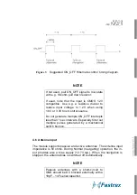
Страница 19: ...eration The ON_OFF interrupt is generated by a low high low toggle which should be longer than 62us and less than 1s suggestion is abt 100ms pulse length Input level is CMOS 1 2V compatible Do not gen...

Страница 20: ...source Do not generate multiple ON_OFF interrupts less than 1 sec intervals Especially filter out multiple pulses generated by a mechanical switch bounce 4 6 Antenna input The module supports passive...

Страница 21: ...ault configuration for baud rates and respective protocols can be changed by commands via NMEA or SiRF binary protocols ref II III Any custom configuration stays active as long as supply VDD is active...

Страница 22: ...at 1Hz rate The I O level is CMOS 1 8V compatible 4 9 2 TSYNC GPIO8 Optional input TSYNC input is intended for external time aiding with a special ROM version used for A GPS GPIO8 is available only f...

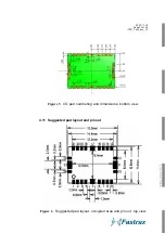
Страница 23: ...2007 11 19 Page 23 of 35 IT321_Tech_doc_12 Figure 5 Figure 6 I O pad numbering and dimensions bottom view 4 11 Suggested pad layout and pin out Suggested pad layout occupied area and pin out top view...

Страница 24: ...mperature is 250C for ten seconds Pb free paste Absolute max reflow temperature is 260C for ten seconds 5 3 Moisture sensitivity Note that the IT321 is moisture sensitive at MSL 3 see the standard IPC...

Страница 25: ...2007 11 19 Page 25 of 35 IT321_Tech_doc_12 Figure 7 Tape and reel specification...

Страница 26: ...olt age specification is not exceeded With a high ripple power supply use an external by pass capacitor s or a low pass filter for VDD sup ply input Serial port TXA is connected to host UART input RXA...

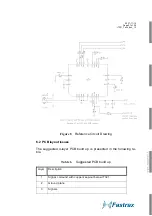
Страница 27: ...re 8 Table 6 Reference Circuit Drawing 6 2 PCB layout issues The suggested 4 layer PCB build up is presented in the following ta ble Suggested PCB build up Layer Description 1 Signal Ground with coppe...

Страница 28: ...e the GND via hole as close as possible to the capacitor Connect the GND soldering pads of the IT321 to ground plane with short traces to via holes which are connected to the ground plane Use preferab...

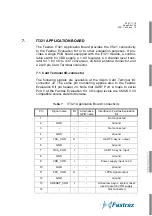
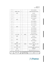
Страница 29: ...e 40 pin Card Terminal I O connector J2 The same pin numbering applies also to the Fastrax Evaluation Kit pin header J4 Note that UART Port A maps to serial Port 0 at the Fastrax Evaluation Kit I O si...

Страница 30: ...6 Not connected 27 Not connected 28 Not connected 29 Not connected 30 UI_A_CON O GPIO1 UI indicator A output 31 GND Ground 32 Not connected 33 GND Ground 34 Not connected 35 GND Ground 36 TIMESYNC_1V8...

Страница 31: ...PCB PCB1 PCB AP321C01 PCB AP321C01 Q1 FDG6321C TRANSISTOR Dual P N FET FDG6321C SOT323 R15 16 N A Resistor chip 0R 0402 R3 R13 14 100k 5 Resistor chip 100k 5 0402 63mW R5 R10 11 R17 R26 27 10k 5 Resis...

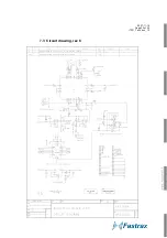
Страница 32: ...2007 11 19 Page 32 of 35 IT321_Tech_doc_12 7 3 Circuit drawing rev C...

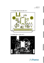
Страница 33: ...2007 11 19 Page 33 of 35 IT321_Tech_doc_12 7 4 Assembly drawing Top side rev C 7 5 Artwork layer 1 Top rev C...

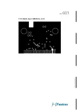
Страница 34: ...2007 11 19 Page 34 of 35 IT321_Tech_doc_12 7 6 Artwork layer 2 rev C 7 7 Artwork layer 3 rev C...

Страница 35: ...2007 11 19 Page 35 of 35 IT321_Tech_doc_12 7 8 Artwork layer 4 Bottom rev C...

Отзывы: