AN-9111
APPLICATION NOTE
© 2015 Fairchild Semiconductor Corporation
www.fairchildsemi.com
Rev. 1.1
• 6/26/15
21
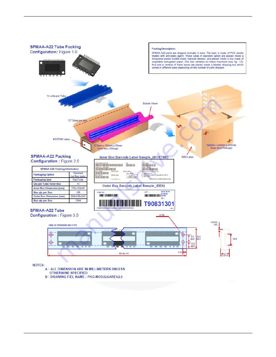
Packing Information
Figure 26.
Страница 1: ...y ON Semiconductor Typical parameters which may be provided in ON Semiconductor data sheets and or specifications can and do vary in different applications and actual performance may vary over time Al...
Страница 2: ...Outline 7 3 4 Marking Specification 8 4 Product Synopsis 9 4 2 Electrical Characteristic TJ 25 o C unless otherwise specified 10 4 3 Recommended Operating Conditions 12 4 4 Mechanical Characteristics...
Страница 3: ...based power module has much better ruggedness and a larger Safe Operation Area SOA than MOSFET based module or Silicon On Insulator modules The FRFET based power module has a big advantage in light l...
Страница 4: ...ine up Table 1 shows the basic line up Online loss temperature simulation tool Motion Control Design Tool Motion Control Design Tool is recommended to find out the right SPM product for the desired ap...
Страница 5: ...the accomplishment of optimization package size while maintaining outstanding heat dissipation characteristics without compromising the isolation rating In the SPM package technology was developed in...
Страница 6: ...NV Negative DC Link Input 7 NU Negative DC Link Input 8 VFO Fault Output 9 IN UL PWM Input for Low Side U Phase MOSFET Drive 10 IN VL PWM Input for Low Side V Phase MOSFET Drive 11 IN WL PWM Input for...
Страница 7: ...built in MOSFETs They are activated by voltage input signals The terminals are internally connected to a Schmitt trigger circuit composed of 5 V class CMOS The signal logic of these pins is active HI...
Страница 8: ...AN 9111 APPLICATION NOTE 2015 Fairchild Semiconductor Corporation www fairchildsemi com Rev 1 1 6 26 15 7 3 3 Package Outline...
Страница 9: ...AN 9111 APPLICATION NOTE 2015 Fairchild Semiconductor Corporation www fairchildsemi com Rev 1 1 6 26 15 8 3 4 Marking Specification...
Страница 10: ...calculation value or design factor Table 4 Control Part Symbol Parameter Conditions Rating Unit VCC Control Supply Voltage Applied between VCC COM 20 V VBS High Side Control Bias Voltage Applied betwe...
Страница 11: ...VBS 15 V VIN 5 V ID 40 A 3 0 4 1 m VSD Source Drain Diode Forward Voltage VCC VBS 15 V VIN 0 V ISD 40 A 0 8 1 1 V HS tON Switching Times VPN 20 V VCC VBS 15 V ID 40 A VIN 0 V 5 V Inductive Load See Fi...
Страница 12: ...8 Control Part Symbol Parameter Conditions Min Typ Max Unit IQCC Quiescent VCC Supply Current VCC H 15 V IN UH VH WH 0 V VCC H COM 2 75 mA IQBS Quiescent VBS Supply Current VBS 15 V IN UH VH WH 0 V VB...
Страница 13: ...WH COM VCC L COM 13 5 15 0 16 5 VBS High Side Bias Voltage Applied between VB U VS U VB V VS V VB W VS W 13 0 15 0 18 5 V dVCC dt dVBS dt Control Supply Variation 1 1 V s VSEN Voltage for Current Sen...
Страница 14: ...and carrying current The HVIC has an under voltage lockout function to protect the high side MOSFET from insufficient gate driving voltage A timing chart for this protection is shown in Figure 11 A f...
Страница 15: ...03 V max 0 033 V Tolerance 10 depends on system Shunt resistance ISC max VSC max RSHUNT min RSHUNT min VSC max ISC max If the deviation of the shunt resistor is limited below 1 RSHUNT typ RSHUNT min...
Страница 16: ...max 60 A and VREF level is 2 5 V To prevent malfunction it is recommended that an RC filter be inserted at the CSC pin To shut down MOSFETs within 3 s when over current situation occurs a time constan...
Страница 17: ...e HVIC does not drive the high side MOSFET if the VBS voltage drops below a specified voltage refer to the datasheet This function prevents the MOSFET from operating in a high dissipation mode There a...
Страница 18: ...21 and Figure 22 shows waveform initial bootstrap capacitor charging voltage and current Figure 21 Each Part Initial Operating Waveform of Bootstrap Circuit Conditions VDC 20 V VCC 15 V CBS 22 F LS M...
Страница 19: ...ootstrap capacitor If the minimum ON pulse width of low side MOSFET or the minimum OFF pulse width of high side MOSFET is tO the bootstrap capacitor must be charged to increase the voltage by V during...
Страница 20: ...BS CSP15 5V RPF Motor VDC CDCS Gating UH Gating VH Gating WL Gating VL Gating UL CPF M C U RSH Current Sensing RS RS RS RS RS RS RBS DBS RBS DBS LVIC VFO VCC IN UL IN VL IN WL COM OUT UL OUT VL OUT WL...
Страница 21: ...D and Power GND as short as possible Place sunbber capacitor between P and N and closely to terminals Isolation distance between high voltage block and low voltage block should be kept The V IN RC fil...
Страница 22: ...AN 9111 APPLICATION NOTE 2015 Fairchild Semiconductor Corporation www fairchildsemi com Rev 1 1 6 26 15 21 Packing Information Figure 26 Packing Information...
Страница 23: ...LICY FAIR HI D PRODU T ARE NOT AUTHORIZED FOR U E A RITI A OMPONENT IN IFE UPPORT DEVI E OR Y TEM WITHOUT THE EXPRESS WRITTEN APPROVAL OF THE PRESIDENT OF FAIRCHILD SEMICONDUCTOR CORPORATION As used h...
Страница 24: ...the rights of others ON Semiconductor products are not designed intended or authorized for use as a critical component in life support systems or any FDA Class 3 medical devices or medical devices wit...