


AN-9111
APPLICATION NOTE
© 2015 Fairchild Semiconductor Corporation
www.fairchildsemi.com
Rev. 1.1
• 6/26/15
16
as the input signals. It is also recommended that the de-
coupling capacitors be placed at both the MCU and Motion-
SPM ends of the VFO and the signal line as close as
possible to each device. The RC coupling at each input
(parts shown dotted in Figure 17 might change depending
on the PWM control scheme used in the application and the
wiring impedance of the application’s PCB layout.
5V-Line
IN
(UH)
, IN
(VH)
, IN
(WH)
IN
(UL)
, IN
(VL)
, IN
(WL)
VF
COM
R
PF
=10k
Ω
C
PF
=1nF
Motion SPM 45L
MCU
Gate
Driver
Level-Shift
Circuit
Typ. 5 k
Input
Noise
Filter
Input
Noise
Filter
Gate
Driver
Typ. 5 k
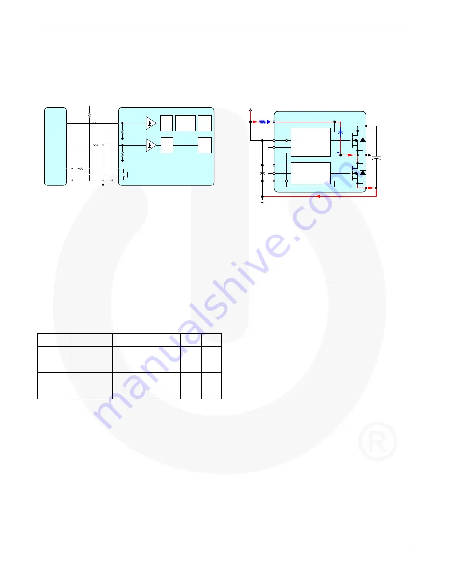
Figure 17. Recommended CPU I/O Interface Circuit
The µMini DIP family of Motion-SPM products employs
active-HIGH input logic. This removes the sequence
restriction between the control supply and the input signal
during startup or shutdown operation. Therefore, it makes
the system fail-safe. In addition, pull-down resistors are
built-in to each input circuit. External pull-down resistors
are not needed, reducing external components. The input
noise filter inside the Motion-SPM product suppresses short
pulse noise and prevents the MOSFET from malfunction
and excessive switching loss. Furthermore, by lowering the
turn-on and turn-off threshold voltages of the input signal,
as shown in
Error! Reference source not found.
, a direct
connection to 3.3 V-class MCU or DSP is possible.
Table 10.
Input Threshold Voltage Ratings
(V
DD
=15 V, T
J
=25°C)
Symbol
Item
Condition
Min. Max. Unit
V
IN(ON)
Turn-On
Threshold
Voltage
IN
(UH)
, IN
(VH)
,
IN
(WH)
-COM
2.6
V
V
IN(OFF)
Turn-Off
Threshold
Voltage
IN
(UL)
, IN
(VL)
,
IN
(WL)
-COM
0.8
V
6.4. Bootstrap Circuit Design
6.4.1.
Operation of Bootstrap Circuit
The V
BS
voltage, which is the voltage difference between
V
B(U,V,W)
and V
S(U,V,W)
, provides the supply to the HVIC
within the motion SPM
®
45 LV series. This supply must be
in the range of 13.0 V~18.5 V to ensure that the HVIC can
fully drive the high-side MOSFET. The SPM 45 LV series
includes an under-voltage lock out protection function for
the V
BS
to ensure that the HVIC does not drive the high-side
MOSFET, if the V
BS
voltage drops below a specified
voltage (refer to the datasheet). This function prevents the
MOSFET from operating in a high dissipation mode.
There are a number of ways in which the V
BS
floating
supply can be generated. One of them is the bootstrap
method described here (refer to Figure 18). This method has
the advantage of being simples and inexpensive. However,
the duty cycle and on-time are limited by the requirement to
refresh the charge in the bootstrap capacitor. The bootstrap
to ground (either through the low-side or the load), the
bootstrap capacitor (C
BS
) is charged through the bootstrap
diode (D
BS
) and the resistor (R
BS
) from the V
CC
supply.
V
S
HVIC
LVIC
V
DC
V
CC(L)
V
B
V
CC(H)
V
CC
IN
(L)
C
BS
C
VCC
Motion-SPM
TM
D
BS
COM
V
CC
COM
H
O
H
O
V
SL
COM
V
CC
V
BS
IN
(H)
IN
(H)
IN
(H)
OFF
ON
V
B
R
BS
Figure 18.
Current path of Bootstrap Circuit
6.4.2.
Selection of Bootstrap Capacitor
Considering Initial Charging
Adequate on-time of the low-side MOSFET to fully charge
the bootstrap capacitor is required for initial bootstrap
charging. The initial charging time (t
charge
) can be calculated
by:
t
charge
R
ln
V
V
V
min
V
F
V
where:
V
F
= Forward voltage drop across the bootstrap diode;
V
BS(min)
=The minimum value of the bootstrap capacitor;
V
LS
= Voltage drop across the low-side MOSFET or load;
and
Duty ratio of PWM
When the bootstrap capacitor is charged initially; V
CC
drop
voltage is generated based on initial charging method, V
CC
line SMPS output current, V
CC
source capacitance, and
bootstrap capacitance. If V
CC
drop voltage reaches UV
CCD
level, the low side is shut down and a fault signal is
activated.
To avoid this malfunction, the related parameter and initial
charging method should be considered. To reduce V
CC
voltage drop at initial charging, a large V
CC
source capacitor
and selection of optimized low-side turn-on method are
recommended. Adequate on-time duration of the low-side
MOSFET to fully charge the bootstrap capacitor is initially
required before normal operation of PWM starts.
Figure 19 shows an example of initial bootstrap charging
sequence. Once V
CC
establishes, V
BS
needs to be charged by
turning on the low-side MOSFETs. PWM signals are
typically generated by an interrupt triggered by a timer with
a fixed interval, based on the switching carrier frequency.


