ES1652.2 Carrier Board for Signal Conditioning Circuits - User’s Guide
6
Introduction
ETAS
The functions of the ES1652.2 Carrier Board for Signal Conditioning Circuits are
shown in the following block diagram:
Fig. 1-2
Block Diagram
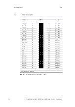
The input signals are supplied via the 9-pin "IN 1..9" connector and routed to
the piggyback. From there, they are led back through connector "OUT 1..15" -
once they have been processed. There are also eight LEDs on the front panel
which can be addressed by the piggyback.
Up to four DC/DC converters can be installed on the ES1652.2 Carrier Board to
power the piggyback. These can be supplied with 5 V or +12 V from the
VMEbus backplane.
There are three fuses on the carrier board that provide protection against volt-
ages from the backplane.
CAUTION!
There is no protective circuit on the ES1652.2 Carrier Board for the
inputs and outputs! If required, this must be ensured by the customer
on the relevant piggyback.
Piggyback
Module
IN
1
..9
OU
T 1..
15
DC/DC Converter
DC/DC Converter
DC/DC Converter
DC/DC Converter
Содержание ES1652.2
Страница 1: ...ES1652 2 Carrier Board for Signal Conditioning Circuits User s Guide...
Страница 4: ...ES1652 2 Carrier Board for Signal Conditioning Circuits User s Guide 4 Contents ETAS...
Страница 12: ...ES1652 2 Carrier Board for Signal Conditioning Circuits User s Guide 12 Hardware Description ETAS...
Страница 16: ...ES1652 2 Carrier Board for Signal Conditioning Circuits User s Guide 16 Technical Data ETAS...
Страница 18: ...ES1652 2 Carrier Board for Signal Conditioning Circuits User s Guide 18 ETAS Contact Addresses ETAS...
Страница 20: ...ES1652 2 Carrier Board for Signal Conditioning Circuits User s Guide 20 Index ETAS...


