Page 22 total 3
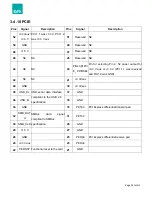
3.4.10 PCIE
Pins Signal
Description
Pins
Signal
Description
52
+3.3Vaux/
+3.3 V
PCI 1.1 was +3.3 V, PCI 1.2
was +3.3 V aux
51
Reserved
NC
50
GND
49
Reserved NC
48
+1.5 V
47
Reserved NC
46
NC
NC
45
Reserved NC
44
NC
NC
43
PIN43_MPCI
E_ PWRSEL
Pin for selecting Pin 2; 52 power output for
+3.3 V aux or +3.3 V (PCI 1.1 was reserved
and PIC1.2 was GND)
42
NC
NC
41
+3.3Vaux
40
GND
39
+3.3Vaux
38
USB_D+ USB serial data interface
compliant to the USB 2.0
specification
37
GND
36
USB_D-
35
GND
34
GND
33
PETp0 PCI Express differential transmit pair
32
SMB_DAT
A
SMBus
data
signal
compliant to SMBus
specification
31
PETn0
30
SMB_CLK
29
GND
28
+1.5 V
27
GND
26
GND
25
PERp0 PCI Express differential receive pair
24
+3.3V aux
23
PERn0
22
PERST# Functional reset to the card
21
GND


