8. APPLIED CIRCUIT EXAMPLES
S1F76640 Technical Manual (Rev.1.5)
EPSON
25
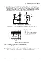
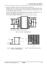
(9) Example of Configuration of Booster Circuits of High Magnification Using Diode
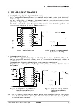
Adding an external diode to the S1F76640 provides quintuple or higher boosting operation and voltage
stabilization output. It is recommended to use the diode of smaller V
F
as the output impedance of the
boosting output increases due to the influence of drop of forward voltage V
F
of the diode. V
DD
= 4V and
V
F
= 0.6V results in output shown in Fig.8.22.
Fig.8.21 shows an example of circuit configuration that provides boosting by 6x magnification using two
diodes and voltage stabilization output. Use the shortest possible wire between V
O
and VRI.
Fig.8.22 shows the diagram of voltage relations.
Use the voltage to be applied to the VRI pin at or below the absolute maximum rated voltage.
1
2
3
4
5
6
7
8
9
10
11
12
13
14
15
16
OSC2
OSC1
V
SS
XP
OFF
TC2
TC1
V
REG
RV VRI
V
O
CAP1
+
CAP1
−
CAP2
−
CAP2
+
CAP3
+
V
DD
C4
10
μ
F
R
OSC
1M
Ω
C1
10
μ
F
C2
10
μ
F
C3
10
μ
F
V
DD
R2
R1
+
−
C7
10
μ
F
V
REG
V
SS
R
RV
1M
Ω
C6
10
μ
F
C5
10
μ
F
V
OUT
A
R
L
I
O
V
OUT
’
D1
D2
+
−
+
−
+
−
+
−
+
−
+
−
(For pins 3 and 4, select any temperature gradient.)
Fig.8.21 Boosters of High Magnification
10
15
20
25
0
5
10
15
20
I
O
[mA]
V
O
' [V]
Ta=25
°
C
V
SS
(0V)
V
DD
(
+
4V)
V
OUT
(
+
16V)
4
$
V
DD
6
$
V
DD
6
$
V
DD
−
2
$
V
F
2
$
V
F
V
OUT
’ (
+
22.8V)
Fig.8.22 Diagram of Voltage Relations of Fig.8.23 Output Voltage - Output Current
Boosters of High Magnification

