

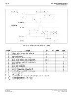
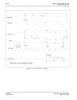


Page 58
Epson Research and Development
Vancouver Design Center
S1D13704
Hardware Functional Specification
X26A-A-001-04
Issue Date: 01/02/08
bit 7
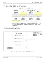
Look-Up Table Bypass
When the Look-Up Table Bypass bit = 0, the Green Look-Up Table is used for display
data output in gray shade modes. When this bit = 1, the Look-Up Table is bypassed for dis-
play data output in gray shade modes (for power save purposes). See “Look-Up Table
Architecture” on pag e72.
There is no effect on changing this bit in color modes. In color display mode the Look-Up
Table cannot be bypassed.
bit 3
LCDPWR Override
This bit is used to override the panel on/off sequencing logic. When this bit = 0, LCDPWR
and the panel interface signals are controlled by the sequencing logic. When this bit 1,
LCDPWR is forced to off and the panel interface signals are forced low immediately upon
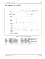
entering power save mode. See Section 7.3.2, “Power Down/Up Timing” on page 36 for
further information.
bit 2
Hardware Power Save Enable
When this bit = 1 GPIO0 is used as the Hardware Power Save input pin. When this bit = 0
GPIO0 operates normally.
bits 1-0
Software Power Save Bits [1: 0]
These bits select the Power Save Mode as shown in the following table.
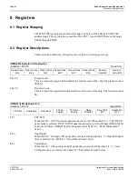
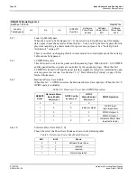
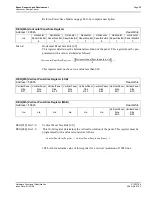
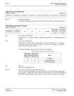
REG[03h] Mode Register 2
Address = FFE3h
Read/Write
Look-Up
Table Bypass
n/a
n/a
n/a
LCDPWR
Override
Hardware
Power Save
Enable
Software
Power Save
Bit 1
Software
Power Save
Bit 0
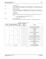
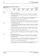
Table 8-5: Hardware Power Save/GPIO0 Operation
RESET#
State
Hardware Power
Save Enable
REG[03h] bit 2
GPIO0 Config
REG[18h] bit 0
GPIO0
Status/Control
REG[19h] bit 0
GPIO0 Operation
0
X
X
X
1
0
0
reads pin status
GPIO0 Input
(high impedance)
1
0
1
0
GPIO0 Output = 0
1
0
1
1
GPIO0 Output = 1
1
1
X
X
Hardware Power Save
Input (active high)
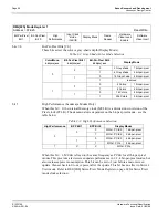
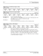
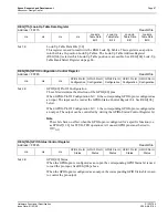
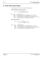
Table 8-6: Software Power Save Mode Selection
Bit 1
Bit 0
Mode
0
0
Software Power Save
0
1
reserved
1
0
reserved
1
1
Normal Operation
*


