


Page 12
Epson Research and Development
Vancouver Design Center
S1D13704
Interfacing to the PC Card Bus
X26A-G-009-03
Issue Date: 01/02/12
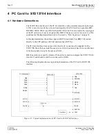
4 PC Card to S1D13704 Interface
4.1 Hardware Connections
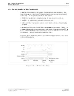
The S1D13704 is interfaced to the PC Card interface with a minimal amount of glue logic.
A PAL is used to decode the write and read signals of the PC Card bus to generate RD#,
RD/WR#, WE0#, WE1#, and CS# for the S1D13704. The PAL also inverts the reset signal
of the PC card since it is active high and the S1D13704 uses an active low reset. For PAL
equations for this implementation refer to Section 4.3, “PAL Equations” on page 14.
In this implementation, the address inputs (AB[15:0]) and data bus (DB[15:0] connect
directly to the CPU address (A[15:0]) and data bus (D[15:0]).
The PC Card interface does not provide a bus clock, so one must be supplied for the
S1D13704. Since the bus clock frequency is not critical, nor does it have to be synchronous
to the bus signals, it may be the same as CLKI.
BS# (bus start) is not used by Generic #1 mode but is used to configure the S1D13704 for
Generic #1 and should be tied low (connected to GND).
The following diagram shows a typical implementation of the PC Card to S1D13704
interface.
Figure 4-1: Typical Implementation of PC Card to S1D13704 Interface
RD/WR#
RD#
DB[15:0]
WAIT#
BUSCLK
S1D13704
RESET#
AB[15:0]
OE#
D[15:0]
WAIT#
A[15:0]
PC Card socket
15K pull-up
PAL16L8-15
CLKI
Oscillator
WE1#
WE0#
CS#
WE#
CE1#
CE2#
REG#
RESET
*


