www.agelectronica.com www.agelectronica.com
www.agelectronica.com www.agelectronica.com
Enfora Enabler IIIG M2M
Modem Integration Guide
4.6.1. Advanced tips for an RF friendly layout
4.6.1.1. Ground Plane
To ensure the lowest possible EMI emissions and maximum thermal conductivity, it is
recommended that all metal tabs on the GSM module shield must be soldered down onto a
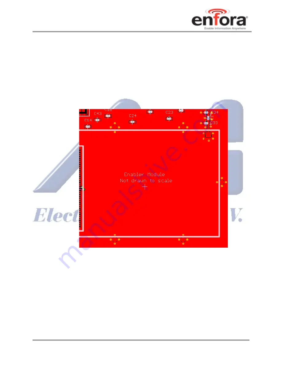
continuous ground plane that runs under the entire module. Ample ground vias should be
provided around the metal tabs to create a low impedance ground. It is recommended to
minimize the number of I/O and power traces and vias under the GSM module to allow for as
much ground plane as possible. An example of a good ground structure and pad layout is
shown below in Figure 1.
Figure 1 - Example of good ground plane for GSM modules
4.6.1.2. Thermal Relief
Because the ground plane acts as a large heat sink, it can affect the solderability of
components. A common method to reduce this effect is to use thermal relief around the pad
in question. However, great care must be taken when using thermal relief for high current or
high frequency applications
For example, a large thermal relief like the one shown in Figure 2 can serve the purpose for
general applications such as low current, low speed data lines, DC connections and audio
GSM0308IG002
15
Version 1.05 – 11/13/08


