

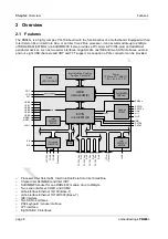


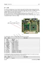

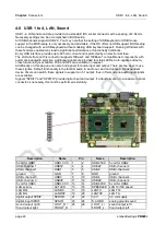


Chapter:
Connectors
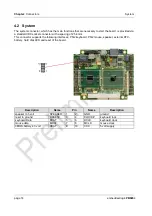
Memory
page 16 embedded-logic
PB945+
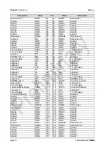
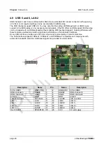
Description
Name
Pin
Name
Description
data strobe 2 +
DQS2
51
52
DQM2
data mask 2
ground
GND
53
54
GND
ground
data 18
DQ18
55
56
DQ22
data 22
data 19
DQ19
57
58
DQ23
data 23
ground
GND
59
60
GND
ground
data 24
DQ24
61
62
DQ28
data 28
data 25
DQ25
63
64
DQ29
data 29
ground
GND
65
66
GND
ground
data mask 3
DQM3
67
68
DQS3#
data strobe 3 -
reserved
N/C
69
70
DQS3
data strobe 3 +
ground
GND
71
72
GND
ground
data 26
DQ26
73
74
DQ30
data 30
data 27
DQ27
75
76
DQ31
data 31
ground
GND
77
78
GND
ground
clock enables 0
CKE0
79
80
CKE1
clock enables 1
1.8 volt supply
1.8V
81
82
1.8V
1.8 volt supply
reserved
N/C
83
84
N/C
reserved
SDRAM bank 2
BA2
85
86
N/C
reserved
1.8 volt supply
1.8V
87
88
1.8V
1.8 volt supply
address 12
A12
89
90
A11
address 11
address 9
A9
91
92
A7
address 7
address 8
A8
93
94
A6
address 6
1.8 volt supply
1.8V
95
96
1.8V
1.8 volt supply
address 5
A5
97
98
A4
address 4
address 3
A3
99
100
A12
address 2
address 1
A1
101
102
A0
address 0
1.8 volt supply
1.8V
103
104
1.8V
1.8 volt supply
address 10
A10
105
106
BA1
SDRAM bank 1
SDRAM bank 0
BA0
107
108
RAS#
row address strobe
write enable
WE#
109
110
S0#
chip select 0
1.8 volt supply
1.8V
111
112
1.8V
1.8 volt supply
column address strobe
CAS#
113
114
ODT0
on die termination 0
chip select 1
S1#
115
116
A13
address 13
1.8 volt supply
1.8V
117
118
1.8V
1.8 volt supply
on die termination 1
ODT1
119
120
N/C
reserved
ground
GND
121
122
GND
ground
data 32
DQ32
123
124
DQ36
data 36
data 33
DQ33
125
126
DQ37
data 37
ground
GND
127
128
GND
ground
data strobe 4 -
DQS4#
129
130
DQM4
data mask 4
data strobe 4 +
DQS4
131
132
GND
ground
ground
GND
133
134
DQ38
data 38
data 34
DQ34
135
136
DQ39
data 39
data 35
DQ35
137
138
GND
ground
ground
GND
139
140
DQ44
data 44
data 40
DQ40
141
142
DQ45
data 45
data 41
DQ41
143
144
GND
ground
ground
GND
145
146
DQS5#
data strobe 5 -
data mask 5
DQM5
147
148
DQS5
data strobe 5 +
ground
GND
149
150
GND
ground
data 42
DQ42
151
152
DQ46
data 46
data 43
DQ43
153
154
DQ47
data 47
ground
GND
155
156
GND
ground
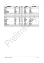
data 48
DQ48
157
158
DQ52
data 52


