


embedded-logic GmbH Telefon: +49 (0) 8075 91-4400
Am Kroit 25-27 Fax: +49 (0) 8075 91-4409
83123 Amerang email: [email protected]
Germany
web:
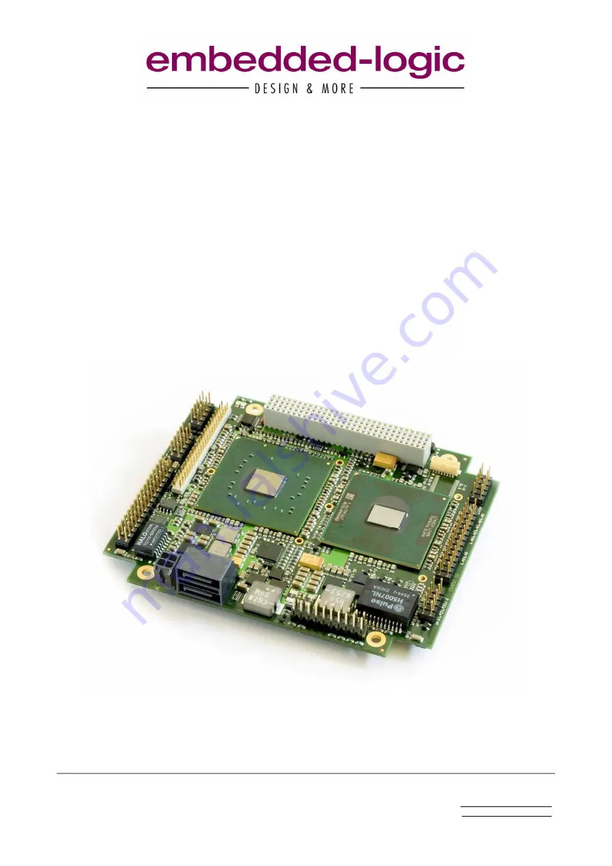
PB945+
Manual
rev 0.2 (preliminary)