Quantum SBC User Manual Rev A
www.diamondsystems.com
Page 41
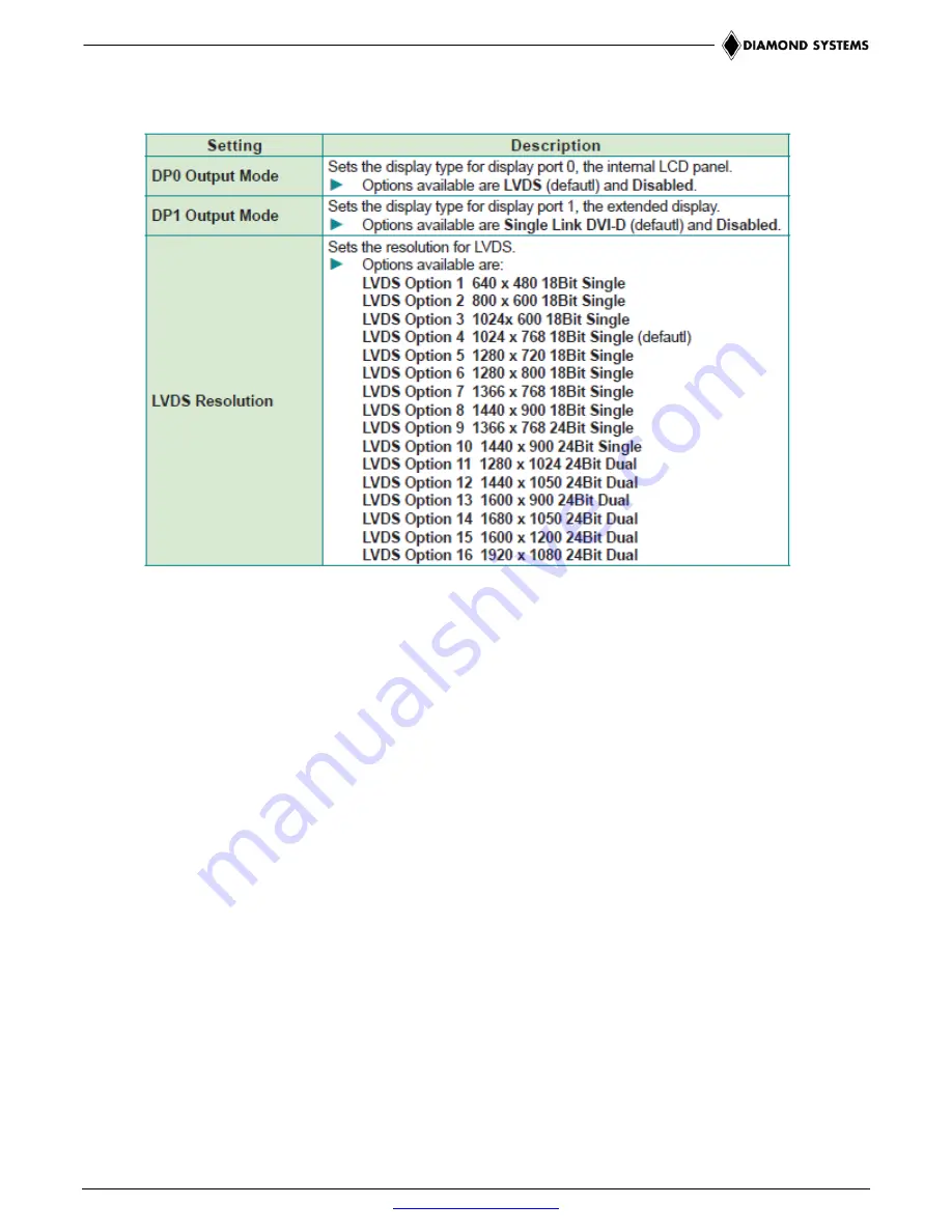
North Bridge LVDS configuration Select
This submenu features the following settings to configure the INT15 options for the LVDS:
South Bridge
Select this submenu to view the so
uth bridge’s CIM version and to configure its features.


