background image

12

DVD-2500BT

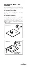
Instructions for Handling Semi-
conductors

Electrostatic breakdown of the semi-conductors may
occur due to a potential difference caused by
electrostatic charge during unpacking or repair work.

1. Ground for Human Body

Be sure to wear a grounding band (1 M

Ω

) that is

properly grounded to remove any static electricity that
may be charged on the body.

2. Ground for Workbench

Be sure to place a conductive sheet or copper plate
with proper grounding (1 M

Ω

) on the workbench or

other surface, where the semi-conductors are to be
placed. Because the static electricity charge on
clothing will not escape through the body grounding
band, be careful to avoid contacting semi-conductors
with your clothing.

<Incorrect>

CBA

Grounding Band

Conductive Sheet or
Copper Plate

1M

Ω

1M

Ω

<Correct>

CBA

Содержание DVD-2500BT

Страница 1: ...ing to the operating instructions without fail Some illustrations using in this service manual are slightly different from the actual set 注 意 サービスをおこなう前に このサービスマニュアル を必ずお読みください 本機は 火災 感電 けが などに対する安全性を確保するために さまざまな 配慮をおこなっており また法的には 電気用品安 全法 にもとづき 所定の許可を得て製造されてお ります 従ってサービスをおこなう際は これらの 安全性が維持されるよう このサービスマニュアル に記載されている注意事項を必ずお守りください 本機の仕様は性能改良のため 予告なく変更すること があります 補修用性能部品の保有期間は 製造打切後 8 年です 修理の際は 必ず取扱...

Страница 2: ... unit to the customer make sure you make either 1 a leakage current check or 2 a line to chassis resistance check If the leakage current exceeds 0 5 milliamps or if the resistance from chassis to either side of the power cord is less than 460 kohms the unit is defective LASER RADIATION Caution Class 1M visible and invisible laser radiation when open Do not view directly with optical instruments Pl...

Страница 3: ...3 DVD 2500BT DIMENSION ...

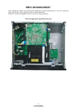
Страница 4: ...wed from the top If wire bundles are untied or moved to perform adjustment or parts replacement etc be sure to rearrange them neatly as they were originally bundled or placed afterward Otherwise incorrect arrangement can be a cause of noise generation ...

Страница 5: ...5 DVD 2500BT SPECIFICATIONS ...

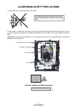
Страница 6: ...ickup lens when the diode is turned on Do not look directly at the laser beam CAUTION Use of controls and adjustments or doing procedures other than those specified herein may result in hazardous radiation exposure Location Inside Top of BD mechanism Do not look directly at the laser beam coming from the pickup or allow it to strike against your skin Drive Mechanism Assembly Laser Beam Radiation L...

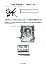
Страница 7: ... is turned on Do not look directly at the laser beam CAUTION Use of controls and adjustments or doing procedures other than those specified herein may result in hazardous radiation exposure Location Top of BD mechanism Do not look directly at the laser beam coming from the pickup or allow it to strike against your skin Drive Mechanism Assembly Laser Beam Radiation Laser Pickup Turntable LASER RADI...

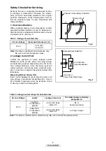
Страница 8: ...le parts RF termi nals antenna terminals video and audio input and output terminals microphone jacks earphone jacks etc is lower than or equal to the specified value in the table below Measuring Method Power ON Insert load Z between B earth ground power cord plug prongs and exposed accessible parts Use an AC voltmeter to measure across the terminals of load Z See Fig 2 and the following table AC L...

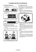
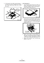
Страница 9: ...achine then apply hot air to the Flat Pack IC about 5 to 6 seconds Fig S 1 1 2 Remove the flat pack IC with tweezers while applying the hot air 3 Bottom of the flat pack IC is fixed with glue to the CBA when removing entire flat pack IC first apply soldering iron to center of the flat pack IC and heat up Then remove glue will be melted Fig S 1 6 4 Release the flat pack IC from the CBA using tweeze...

Страница 10: ... by one using a sharp pin or wire to which solder will not adhere iron wire When heating the pins use a fine tip soldering iron or a hot air desoldering machine Fig S 1 4 3 Bottom of the flat pack IC is fixed with glue to the CBA when removing entire flat pack IC first apply soldering iron to center of the flat pack IC and heat up Then remove glue will be melted Fig S 1 6 4 Release the flat pack I...

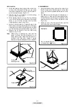
Страница 11: ...rs Fig S 1 6 Note When using a soldering iron care must be taken to ensure that the flat pack IC is not being held by glue When the flat pack IC is removed from the CBA handle it gently because it may be damaged if force is applied 2 Installation 1 Using desoldering braid remove the solder from the foil of each pin of the flat pack IC on the CBA so you can install a replacement flat pack IC more e...

Страница 12: ...ed to remove any static electricity that may be charged on the body 2 Ground for Workbench Be sure to place a conductive sheet or copper plate with proper grounding 1 MΩ on the workbench or other surface where the semi conductors are to be placed Because the static electricity charge on clothing will not escape through the body grounding band be careful to avoid contacting semi conductors with you...

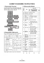
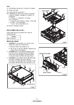
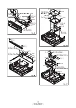
Страница 13: ...Assembly 8 Front Bracket 2 Top Panel 14 RS232C CBA 16 AV CBA 18 Pedestal 15 Power Supply CBA 17 Sub Microcontroller CBA 9 Rear Panel 10 BE Main CBA Unit 11 FE Main CBA BD Mechanism Assembly 13 Motor DC Fan 5 Front CBA 12 Fan Holder ID Loc No Part Removal Fig No Remove Unhook Unlock Release Unplug Desolder Note 1 Top Cover D1 9 S 1 2 S 2 2 Top Panel D2 10 S 3 3 Tray Panel D3 2 L 1 1 4 Front Assembl...

Страница 14: ... 1 Locking Tabs L 1 and L 2 are fragile Be careful not to break them 1 Release three Locking Tabs L 2 2 Disconnect connectors CN2001 CN4002 then remove the Front Assembly 2 CAUTION 2 When installing the BE Main CBA Unit with a screw hold and press the BE Main CBA Unit to align the HDMI connector with the connector s hole for HDMI on the Rear Panel 3 CAUTION 3 The FE Main CBA BD Mechanism Assembly ...

Страница 15: ...0 S 11 S 12 S 13 S 14 S 15 S 15 S 15 CN1003 9 Rear Panel 8 Front Bracket S 9 S 9 Fig D5 S 16 S 16 S 17 S 17 S 17 S 18 S 18 S 18 CN6401 BE Scaler Holder BE Scaler Sub Holder CN7001 CN7401 Mecha Earth Plate Fig D6 10 BE Main CBA Unit S 19 S 19 S 19 S 20 S 20 S 21 CN2500 CN2601 11 FE Main CBA BD Mechanism Assembly 12 Fan Holder 13 Motor DC Fan Fig D7 ...

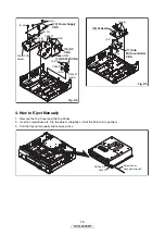
Страница 16: ...tly so that the Portion A is pushed 3 Pull the tray out manually and remove a disc S 22 S 22 S 23 S 24 Power PCB Holder RS232C Holder S 24 S 26 S 26 S 25 CN2551 CN2501 CN2503 Fig D8 14 RS232C CBA 15 Power Supply CBA 16 AV CBA S 27 Wire S 28 Fig D9 17 Sub Microcontroller CBA 18 Pedestal Portion A Hole A Screwdriver hexagon wrench ...

Страница 17: ...DVD 2500BT View from the bottom Cautions concerning the structure The chassis touches the patterns on the circuit board at 6 points but these patterns are all ground patterns so performance is not affected ...

Страница 18: ...ISPLAY buttons on the remote control unit in that order Fig a appears on the screen 3 Press STOP button on the remote control unit Fig b appears on the screen and Fig c appears on the VFD 4 To exit this mode press POWER OFF button Fig a differ depending on the models Model Name Version Region Version Info EXIT POWER EEPROM CLEAR STOP Fig b differ depending on the models Model Name Version Region V...

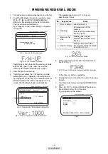
Страница 19: ... available 6 Unplug the AC cord from the AC outlet Then plug it again 7 Turn the power on by pressing the POWER ON button 8 Press 1 2 3 4 and DISPLAY buttons on the remote control unit in that order Fig g appears on the screen F W VERSION UP MODE Model No Ver Please insert a Disc for F W Version Up differs depending on the models Fig a Version Up Mode Screen Fig b VFD in Version Up Mode 1 ALL Now ...

Страница 20: ...ote control unit in that order Fig j appears on the screen 3 To exit this mode press POWER OFF button Fig h differ depending on the models Model Name Version Region Version Info EXIT POWER EEPROM CLEAR STOP EEPROM CLEAR OK Fig i Fig j differ depending on the models Model Name Version Region Version Info EXIT POWER EEPROM CLEAR STOP b The region setting can be changed up to five times including fac...

Страница 21: ...LD 2 BD Turning on BD LD 3 DVD Turning on DVD LD 4 CD Turning on CD LD 2 Operating Time 1 BD Displaying BD LD Operation Time 2 DVD Displaying DVD LD Operation Time 3 CD Displaying CD LD Operation Time 4 STOP Clear LD Operation Total Time When the mechanism is replaced LD Operation Total Time is cleared 5 Channel Level 1 TEST TONE 1 Center Subwoofer Front LR 2 Surround LR Surround Back LR 2 Front L...

Страница 22: ...ig l appears on the VFD Available button in service mode Note Press the number key to select items Or press the cursor button up down to select items and press ENTER button Button condition ENTER Enter the next level POWER Turn the power off when the service mode is completed 1 8 Enter the selected item next level OTHER Not available INDICATION DESCRIPTION REMARK Model Name Model Name E5J D etc Re...

Страница 23: ...h playback stopped press SETUP TOP MENU 3 AUDIO 0 and SETUP buttons on the remote control unit in that order Trade On will appear in the upper right corner on the screen and on VFD for 2 seconds 3 To exit this mode press SETUP TOP MENU 3 AUDIO 0 and SETUP buttons on the remote control unit in that order Trade Off will appear in the upper right corner on the screen and on VFD for 2 seconds Fig a VF...

Страница 24: ...e front panel simultaneously for over 3 seconds to set Remote Lock Mode and display mode 2 Press STILL PAUSE button on the remote control unit to set to On or Off When Remote Lock On Remote Lock On will appear in the upper right corner on the screen and appears on the VFD When Remote Lock Off Remote Lock Off will appear in the upper right corner on the screen and appears on the VFD a If STILL PAUS...

Страница 25: ... service it if defective FLOW CHART NO 5 FL is not outputted Is 30V voltage supplied to the emitter of Q2503 Check D1018 C1021 and periphery circuit and service it if defective Check Q2503 and their periphery and service it if defective Check FL SW line and service it if defective Is the L signal outputted to the collector of Q2507 Yes Yes Yes Yes No No No No No FLOW CHART NO 1 The power cannot be...

Страница 26: ...2601 Yes No FLOW CHART NO 9 P ON 1 2V is not outputted Replace IC2601 Is the voltage of base on Q2610 lower than the voltage of emitter on Q2610 when turning the power on Replace Q2610 Check Q2607 and PWSW3 line and service it if defective Yes No Check D1013 D1014 D1021 C1019 C1025 and their periphery and service it if defective Is 5V voltage inputted to the emitter of Q2606 Yes No Is the voltage ...

Страница 27: ...d Is the H pulse inputted to the Pin 27 of IC2000 Replace IC2000 Is 5V voltage supplied to Pin 2 of RS3000 remote control receiver Yes No Check EV 5V line and service it if defective No No Yes Yes Yes Yes Yes Yes No No No No FLOW CHART NO 11 The fluorescent display tube does not light up Is 3 3V voltage supplied to Pin 64 of IC3001 Is the voltage of approximately 30V supplied to Pin 56 of IC3001 I...

Страница 28: ... poor Replace the FE Main CBA BD Mechanism Assembly No improvement can be found No Yes FLOW CHART NO 14 The disc tray cannot be opened and closed It can be done using the remote control unit Is the normal control voltage inputted to Pin 3 of IC2000 Refer to FLOW CHART NO 12 The key operation is not functioning Refer to FLOW CHART NO 15 The disc tray cannot be opened and closed Replace the OPEN CLO...

Страница 29: ...nism Assembly The upgrading method differs depending on the version of the BD Mechanism Assembly that has been judged defective and the pickup version of the non defective BD Mechanism Assembly Perform according to the following approach BD ROM BLX 201S3 SONY chp12 BD R SBD 8284 ALMEDIO ex Identification code N2008418A3 77D2A00064 7 B1 0 Set Serial No with B1 0 00001 19999 J B1 5 Set Serial No wit...

Страница 30: ... reading data Fig d appears on the screen Select the 4 BE NAND pressing arrow buttons then press ENTER OK button 6 Fig e appears on the screen The appearance shown in 1 of Fig e is described as follows 7 After programming is finished the checksum is displayed on the VFD Fig g At this time no button is available 8 Unplug the AC cord from the AC outlet Then plug it again F W VERSION UP MODE Model No...

Страница 31: ...lug it again No Appearance State 1 Now Loading It means that BD player begin to read the data of the disc 2 Reading Sending files into the memory When BD player finishes reading data it will open a tray automatically 3 Remove the Disc It has finished reading data Please remove the updata disc and close the tray E5H UD A1 bin E5E UD_dummy_ bin differs depending on the models Fig h Firmware Select S...

Страница 32: ...R KEY SWITCH KEY SWITCH 27 20 34 33 44 55 43 M3 Q2004 BUFFER LED DRIVE 14 8 9 RESET 48 SUB TXD 49 L3 A16 SUB RXD LED R SYS RESET RDY RDY B18 TXD1 G18 A18 A17 RXD1 SCL SDA SCL SDA FL SDA FL SCL FL CS REMOTE KEY 1 3 KEY 2 OSC2 OSC1 8MHz X TAL X2000 EV 3 3V IC2001 RESET D 3 3V D 3 3V Q2000 54 LED DRIVE LED G Q2001 Q6702 Q6703 Q6701 10 25 RS232C RXD 9 26 RS232C TXD 14 21 REMOTE 19 RS232C RXD 18 RS232C...

Страница 33: ...EQ AG28 AH4 AG5 U4 U3 T2 R3 T1 R4 AA1 Y3 K4 100 125 128 AH29 AH28 AH30 2 4 7 9 10 11 12 13 14 SLD2 4 SLD2 3 SLD1 2 SLD1 1 CN902 LOAD 5 LOAD 6 LDSNS1 2 LDSNS2 1 CN901 TD 3 TR 4 FD1 1 FR1 2 EXPA 9 EXPA 7 EXPB 10 EXPB 8 A D 21 24 E H 26 29 OEVC 25 RF 17 RF 18 BDRF 14 BDRF 15 SDATA 40 SCLK SDATA SCLK SDATA SCLK 38 CN101 CN101 15 16 17 18 14 13 12 11 14 13 15 16 LOADING MOTOR DRIVE 10 9 COLLIMATE LENS ...

Страница 34: ...it x 4 3 18 IDE1D 0 15 13 13 SDDAT0 15 15 SDDAT1 1 1 SDDAT2 3 3 SDDAT3 11 11 SDCLK 7 7 SDCD DDR SDRAM IC6507 IC6508 IC6509 IC6510 DDR SDRAM 512Mbit x 4 D33 D34 E32 E34 F32 F34 G30 G32 H29 H30 H32 J28 J30 A8 A9 A11 B8 B10 B11 C11 E12 E13 F14 G13 G14 A10 A12 A13 B9 B12 B13 C10 C12 E14 F13 F15 G15 A27 B27 F26 G26 GRAPHICS OSD PIXEL DATA I F CLK VS HS 16 16 SDWP SD CLOCK SD DATA 0 3 SD CARD DETECT SD ...

Страница 35: ...DATA2 T M D S DATA1 T M D S DATA1 T M D S DATA0 T M D S DATA0 T M D S CLOCK T M D S CLOCK JK7501 HDMI CONNECTOR DDC DATA DDC CLOCK HOT PLUG DETECT IC7501 HDMI INTERFACE 6 4 9 7 10 12 3 1 15 19 16 IC7502 Q7505 Q7506 3 3V 5V CONVERTER 6 5 2 3 46 45 44 42 41 39 36 35 DRIVE 23 25 19 21 15 17 13 11 113 116 118 120 119 VIDEO SIGNAL AUDIO SIGNAL 121 83 84 CLK VS HS REGISTER IIC I F DDC I F AUTHENT CATION...

Страница 36: ...07 Q1003 VDD POWER SUPPLY CBA 2 4 7 6 T1001 11 12 15 13 10 9 16 14 AC CORD CN1003 AC INLET F1001 LINE FILTER L1001 3 4 IC1003 ERROR VOLTAGE DET 1 2 SHUNT REG IC2601 IC2600 D1001 D1004 BRIDGE RECTIFIER SWITCHING CONTROL 5 2 3 AL 15V 1 14 16 AL 15V 2 17 19 AL 5V 20 AL 2 5V 23 F1 21 F2 22 FL 12 EV 3 3V 3 14 16 17 19 20 23 21 22 12 CN1001 2 5 AL 5V CN1002 CN2501 FAN VCC 1 2 FAN LOCK CN2500 1 3 P ON 10...

Страница 37: ...stitute replacement parts that do not have the same safety characteristics as specified in the parts list may create shock fire or other hazards Notes 1 Do not use the part number shown on these drawings for ordering The correct part number is shown in the parts list and may be slightly different or amended since these drawings were prepared 2 All resistance values are indicated in ohms K 103 M 10...

Страница 38: ... maintain original function and reliability of repaired units use only original replacement parts which are listed with their part numbers in the parts list section of the service manual 4 Voltage indications for PLAY and STOP mode on the schematics are as shown below 5 How to read converged lines 6 Test Point Information 2 3 1 5 0 2 5 5 0 The same voltage for both PLAY STOP modes Indicates that t...

Страница 39: ...39 DVD 2500BT AV Schematic Diagram SC s ...

Страница 40: ...40 DVD 2500BT Sub Microcontroller Schematic Diagram ...

Страница 41: ...ee that all components in the power supply circuit are not defective before you connect the AC plug to the AC power supply Otherwise it may cause some components in the power supply circuit to fail NOTE The voltage for parts in hot circuit is measured using hot GND as a common terminal CAUTION For continued protection against fire hazard replace only with the same type fuse ...

Страница 42: ...7 P8 P9 FL3000 MATRIX CHART P10 P11 P12 P13 P14 P15 P16 P17 P18 P19 P20 P21 P22 P23 P24 P25 P26 P27 P28 P29 P30 P31 P32 P33 P34 P35 P36 SUPER HD BD PROG RAND B 1 A SD USB NET DVD V CD AUDIO DIGITAL DTS DTS MP3 HDCD x MPEG PCM L P D MIX ANGLE WMA AAC MSTR HD Express TrueHD V S S PL a1 a2 a3 a4 a5 b1 b2 b3 b4 b5 c1 c2 c3 c4 c5 d1 d2 d3 d4 d5 e1 e2 e3 e4 e5 f1 f2 f3 f4 f5 g1 g2 g3 g4 g5 h1 a1 b1 c1 d...

Страница 43: ...43 DVD 2500BT E5J01SCSD RS232C Schematic Diagram E5J01SCRS SD Schematic Diagram ...

Страница 44: ...E Main 1 5 Schematic Diagram The order of pins shown in this diagram is different from that of actual IC001 IC001 is divided into four and shown as IC001 1 4 IC001 4 4 in this FE Main Schematic Diagram Section 1 NOTE ...

Страница 45: ...E Main 2 5 Schematic Diagram The order of pins shown in this diagram is different from that of actual IC001 IC001 is divided into four and shown as IC001 1 4 IC001 4 4 in this FE Main Schematic Diagram Section 1 NOTE ...

Страница 46: ...46 DVD 2500BT FE Main 3 5 Schematic Diagram ...

Страница 47: ...E Main 4 5 Schematic Diagram The order of pins shown in this diagram is different from that of actual IC001 IC001 is divided into four and shown as IC001 1 4 IC001 4 4 in this FE Main Schematic Diagram Section 1 NOTE ...

Страница 48: ...E Main 5 5 Schematic Diagram The order of pins shown in this diagram is different from that of actual IC001 IC001 is divided into four and shown as IC001 1 4 IC001 4 4 in this FE Main Schematic Diagram Section 1 NOTE ...

Страница 49: ...Main 1 9 Schematic Diagram The order of pins shown in this diagram is different from that of actual IC6001 IC6001 is divided into eight and shown as IC6001 1 8 IC6001 8 8 in this BE Main Schematic Diagram Section 2 NOTE ...

Страница 50: ...Main 2 9 Schematic Diagram The order of pins shown in this diagram is different from that of actual IC6001 IC6001 is divided into eight and shown as IC6001 1 8 IC6001 8 8 in this BE Main Schematic Diagram Section 2 NOTE ...

Страница 51: ...Main 3 9 Schematic Diagram The order of pins shown in this diagram is different from that of actual IC6001 IC6001 is divided into eight and shown as IC6001 1 8 IC6001 8 8 in this BE Main Schematic Diagram Section 2 NOTE ...

Страница 52: ...Main 4 9 Schematic Diagram The order of pins shown in this diagram is different from that of actual IC6001 IC6001 is divided into eight and shown as IC6001 1 8 IC6001 8 8 in this BE Main Schematic Diagram Section 2 NOTE ...

Страница 53: ...Main 5 9 Schematic Diagram The order of pins shown in this diagram is different from that of actual IC6001 IC6001 is divided into eight and shown as IC6001 1 8 IC6001 8 8 in this BE Main Schematic Diagram Section 2 NOTE ...

Страница 54: ...Main 6 9 Schematic Diagram The order of pins shown in this diagram is different from that of actual IC6001 IC6001 is divided into eight and shown as IC6001 1 8 IC6001 8 8 in this BE Main Schematic Diagram Section 2 NOTE ...

Страница 55: ...Main 7 9 Schematic Diagram The order of pins shown in this diagram is different from that of actual IC6001 IC6001 is divided into eight and shown as IC6001 1 8 IC6001 8 8 in this BE Main Schematic Diagram Section 2 NOTE ...

Страница 56: ...Main 8 9 Schematic Diagram The order of pins shown in this diagram is different from that of actual IC6001 IC6001 is divided into eight and shown as IC6001 1 8 IC6001 8 8 in this BE Main Schematic Diagram Section 2 NOTE ...

Страница 57: ...57 DVD 2500BT BE Main 9 9 Schematic Diagram ...

Страница 58: ...GND 11 SDCLK 11 NU 10 GND 9 GND 8 GND 7 GND 6 GND 5 AL 5V 4 AL 5V 3 AL 5V 2 AL 5V 1 SAFETY 12 GND 13 SDDAT0 14 GND 15 SDDAT1 16 SDWP 1 2 3 4 5 6 7 8 9 10 11 NU 11 GND 10 GND 9 GND 8 GND 7 GND 6 AL 5V 5 AL 5V 4 AL 5V 3 AL 5V 2 SAFETY 1 12 13 14 15 16 1 NU 2 GND 3 AL 15V 1 4 GND 5 GND 6 NU 7 SAFETY 8 NU 9 GND 10 GND 11 GND 12 EV 3 3V 13 NU 14 AL 15V 2 15 AL 15V 2 16 AL 15V 2 17 AL 5V 18 AL 5V 19 AL ...

Страница 59: ...59 DVD 2500BT MEMO ...

Страница 60: ...L020 2L029 2L019 2L019 2L029 B15 B31 A6 A6 A6 A5 A2 B3 B30 A6 A7 A7 A7 A7 2L021 2L082 2L062 2L062 2L013 B40 2L014 2L014 2L041 2L041 2L027 2L015 2L026 2L060 2L034 2L034 2L022 2L012 2L063 A4 B20 2L081 A21 2L061 2L070 2L080 2L081 2L025 2L081 FRONT CBA POWER SW CBA CN4003 B46 FE MAIN CBA BD MECHANISM ASSEMBLY AV CBA B49 BE MAIN CBA Unit SUB MICROCONTROLLER CBA RS232C CBA SD CBA W10 W05 FN1001 W04 W03 ...

Страница 61: ... E5E00UD 1VM020691S 1 A3 00D9H26000946 TOP COVER E5E00UD BK model 1VM020690 1 A3 00D9H26000927 TOP COVER SILVER E5E02JD SP SR model 1VM223921 1 A4 9H2406000700D REAR PANEL E5J01ED E2 1VM225698 1 A4 9H2406000980D REAR PANEL 1VM226117 DVD2500BTBKE2R E2R 1VM226117 1 A5 nsp BOTTOM PANEL LOW E5E01UD 1VM225238 2 A6 00D1040334007 DENON FOOT E5E00UD 1VM426219 4 A7 00D4611050005 FOOT RUBBER DENON E5E00UD 1...

Страница 62: ... SCREW P TIGHT M3X8 BIND HEAD GBJP3080 2 2L018 nsp SCREW P TIGHT M3X8 BIND HEAD GBJP3080 9 2L019 nsp SCREW P TIGHT M3X8 BIND HEAD GBJP3080 3 2L020 nsp SCREW S TIGHT M3X6 BIND HEAD GBJS3060 8 2L021 nsp SCREW S TIGHT M3X6 BIND HEAD GBJS3060 10 2L022 nsp SCREW S TIGHT M3X6 BIND HEAD GBJS3060 3 2L023 nsp SCREW S TIGHT M3X8 DISH HEAD GDHS3080 2 2L025 nsp SCREW S TIGHT M3X6 BIND HEAD GBJS3060 2 2L026 ns...

Страница 63: ...63 DVD 2500BT PACKING X2 X12 Upper Side Lower Side X15 X6 S3 S5 S8 A22 A30 S2 S5 S6 S4 S4 X4 A30 X1 S9 ...

Страница 64: ...531000730D GIFT BOX CARTON E5J03ED E2 SP model 1VM327703 1 S2 9H2531000740D GIFT BOX CARTON E5J05ED E2 SR model 1VM327704 1 S2 9H2531000960D CARTON 1VM328362 DVD2500BTBKE2R E2R 1VM328362 1 S3 nsp WRAPPING SHEET MIRROR MAT E5E00UD 1VM426159 1 S4 00D9H26000934 TOP SIDE PAD E5E01UD 1VM121561 2 S5 00D9H26000935 BOTTOM SIDE PAD E5E00UD 1VM121380 2 S6 00D9H26000936 FRONT PAD E5E00UD 1VM325022 1 S8 00D9H...

Отзывы: