43
PCM-3362 User Manual
Chapter 4
S
oftware
Introduction
&
Installation
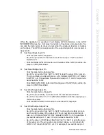
When the application is executed, it will display GPIO information in the GPIO
INFORMATION group box. It displays the number of input pins and output pins. You
can click the radio button to choose to test either the single pin function or multiple
pin functions. The GPIO pin assignments of the supported platforms are located in
Appendix B.
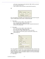
Test Read Single Input Pin
–
Click the radio button- Single-Pin.
–
Key in the pin number to read the value of the input pin. The Pin number
starts from '0'.
–
Click the READ GPIO DATA button and the status of the GPIO pin will be dis-
played in (R/W) Result field.
Test Read Multiple Input Pin
–
Click the radio button- Multiple-Pins.
–
Key in the pin number from ‘0x01’ to ‘0x0F’ to read the value of the input pin.
The pin numbers are ordered bitwise, i.e. bit 0 stands for GPIO 0, bit 1 stands
for GPIO 1, etc. For example, if you want to read pin 0, 1, and 3, the pin num-
bers should be ‘0x0B’.
–
Click READ GPIO DATA button and the statuses of the GPIO pins will be dis-
played in (R/W) Result field.
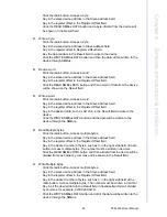
Test Write Single Output Pin
–
Click the radio button- Single-Pin.
–
Key in the pin numbers you want to write. Pin numbers start from '0'.
–
Key in the value either '0' or '1' in (R/W) Result field to write the output pin you
chose above step.
–
Click the WRITE GPIO DATA button to write the GPIO output pin.
Test Write Multiple Output Pins
–
Click the radio button- Multiple-Pins.
–
Key in the pin number from ‘0x01’ to ‘0x0F’ to choose the multiple pin num-
bers to write the value of the output pin. The pin numbers are ordered bit-
wise, i.e. bit 0 stands for GPIO 0, bit 1 stands for GPIO 1, etc. For example, if
you want to write pin 0, 1, and 3, the pin numbers should be ‘0x0B’.
–
Key in the value in (R/W) Result field from ‘0x01’ to ‘0x0F’ to write the value
of the output pin. The pin numbers are ordered bitwise, i.e. bit 0 stands for
GPIO 0, bit 1 stands for GPIO 1, etc. For example, if you want to set pin 0
Содержание PCM-3362
Страница 1: ...Data Modul AG www data modul com Specification PCM 3362 ...
Страница 12: ...5 PCM 3362 User Manual Chapter 1 General Information Figure 1 2 Board layout Dimensions Solder Side ...
Страница 13: ...PCM 3362 User Manual 6 ...
Страница 14: ...Chapter 2 2 Hardware Installation ...
Страница 23: ...PCM 3362 User Manual 16 ...
Страница 24: ...Chapter 3 3 AMI BIOS Setup ...
Страница 44: ...Chapter 4 4 Software Introduction Installation ...
Страница 55: ...PCM 3362 User Manual 48 ...
Страница 56: ...Chapter 5 5 Chipset Software Installation Utility ...
Страница 58: ...Chapter 6 6 Integrated Graphic Device Setup ...
Страница 60: ...Chapter 7 7 LAN Configuration ...
Страница 75: ...PCM 3362 User Manual 68 ...
Страница 76: ...Appendix C C Mechanical Drawings ...
Страница 77: ...PCM 3362 User Manual 70 C 1 Board Mechanical Drawings Figure C 1 PCM 3362 Mechanical Drawing Component Side ...
Страница 78: ...71 PCM 3362 User Manual Appendix C Mechanical Drawings Figure C 2 PCM 3362 Mechanical Drawing Solder Side ...
Страница 81: ...PCM 3362 User Manual 74 ...
Страница 82: ...Appendix D D Watchdog Timer and GPIO sample code ...

