7
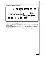
3. GENERAL CIRCUIT OPERATION
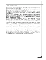
The circuit shown is a highly accurate 38V, 12.5V, 6.0V, -24V, 4.5V, 20W secondary regulated flyback power supply
that will operate from 85V to 265 VAC input voltage.
The input voltage is rectified and filtered by D801 and C1. L801, C801, C804 reduce conducted emissin current.
C806, L801, C805 reduce common mode noises. R801 is ESD path resistor.
Voltage feedback is obtained from the transformer (T11) bias winding, which eliminates the need for optocoupler and
secondary-referenced error amplifier. High-Voltage DC is applied to the primary-high-voltage DC is applied to the
primary-winding of T11.
The other side of the transformer primary is driven by the integrated high-voltage MOS FET-transistor within the
TOP214 (IC11). The circuit operates at a switching frequency of 100KHz, set by the internal oscillator of the TOP
(IC11). The clamp circuit impelemented by DZ11, D11, C17 and R13 limits the leading-edge voltage spike caused by
transformer leakage inductance to a safe value.
The 38V power secondary winding is rectified by DC1, C25. The 12.5V power secondary winding is rectified and
filtered by D24, C24. The 6.0V power secondary winding is rectified and filtered by D23, L22, C23. The -24V power
secondary winding is rectified and filtered by DC2 and C22. The F(+) and F(-) power secondary winding is rectified
and filterd by DC3, C21 and C29.
A IC21(KA431) shunt regulator directly senses and accurately regulates the output voltage. The effective output
voltage can be file turned by adjusting the resistor divider formed by R24, R25 and R26. Other output voltages are
possible by adjusting the transformer turns ratio as well as the divider ratio.
The IC21(KA431) regulates the output voltage by controlling optocoupling LED current (and IC11 duty cycle) to
maintain an average voltage of 2.5V at the IC21 input pin.
Divider R24, R25 and R26 determine the actual output voltage. C27, R27 rolls off the high frequency gain of the
KA31 for stable operation.
R23 limits optocoupler LED current and determines high-frequency loop gain. SPFT start capacitor C26 increases
optocoupler current turn-on to limit the duty cycle and down the risting output voltage. C26 has minimal effect on the
control loop during normal operation. R22 dicharges soft start capacitor C26 when input power is removed.
The output of the T11 bias winding is rectified and filtered by D12, C11 and R11 to create a typical 12V bias voltage
R12, R13 together with the control pin dynamic impedance and capacitor ESR establish a control loop pole-zero pair.
C13, R12 also determines the auto frequency and filters internal gate drive switching current.
CIRCUIT
Содержание DV-K88 series
Страница 71: ...68 CIRCUIT DIAGRAMS 9 1 Connection Diagram SECTION 9 CIRCUIT DIAGRAM 68...
Страница 72: ...69 CIRCUIT DIAGRAMS R819 5 1 9 2 Power Circuit Diagram...
Страница 73: ...70 CIRCUIT DIAGRAMS 9 3 Syscon and Logic Circuit Diagram...
Страница 74: ...71 CIRCUIT DIAGRAMS 9 4 AV SW Circuit Diagram...
Страница 75: ...72 CIRCUIT DIAGRAMS 9 5 IF PDC Circuit Diagram TM...
Страница 76: ...73 CIRCUIT DIAGRAMS 9 6 If Module Circuit Diagram A2...
Страница 77: ...74 CIRCUIT DIAGRAMS 9 7 If Module Circuit Diagram Nicam...
Страница 78: ...75 CIRCUIT DIAGRAMS 9 8 Hi Fi Pre Amp Circuit Diagram...
Страница 79: ...76 CIRCUIT DIAGRAMS 9 9 Video Audio Circuit Diagram...
Страница 80: ...77 CIRCUIT DIAGRAMS 9 10 Remocon Circuit Diagram...
Страница 81: ...SECTION 10 COMPONENTS LOCATION GUIDE ON PCB BOTTOM VIEW 78 P C B LOCATION 10 1 PCB Main...
Страница 82: ...80 P C B LOCATION 10 3 PCB Logic DV K8K S S Series DV K86 S S Series DV K82 S S Series...
Страница 83: ...81 P C B LOCATION DV K88 S S Series...
Страница 84: ...SECTION 11 DISASSEMBLY 83 DISASSEMBLY 11 1 Packing Ass y...
Страница 85: ...84 DIAGRAMS DV K88 Series DV K82 Series DV K8K Series DV K86 Series 11 2 Front Panel Assembly...


