48
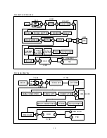
8) The operation of MPX IC (SBX 1837) Hi-Fi Only
!
L + R (MAIN)
MPX signal is input from Pin 39 (COMP IN), and SAP and TELEMETRY signals are suppressed by stereo LPF.
Then, pilot cancel is carried out. Finally L-R and SAP signals are eliminated by MAIN LPF and frequency characteristics are rendered
flat by de-emphasis to be input to the matrix.
@
L – R (SUB)
Up to pilot cancel, the course is the same as for L+R signal. As L–R signal is the amplitude modulation of the double side band quies-
cent carrier (DSB-AM modulation), there is no carrier signal. To this effect the carrier signal (dummy sine wave) is played back using
the pilot signal. As a result L–R signal is demodulated. Finally high band residual components are removed by means of SUB LPF and
L–R signal is input to dbx-TV block through NRSW circuit.
#
SAP
As shown in Fig. 1 SAP is an FM signal with a 5fH carrier. First SAP signal alone is extracted using SAP BPF. This is FM detected.
Finally high band residual components are removed by means of SAP LPF, frequency characteristics are rendered flat and SAP is input
to dbx-TV block through NRSW circuit.
$
Mode discrimination
Stereo discrimination is executed through the detection of the pilot signal amplitude SAP discrimination is executed by means of the
5fH carrier and noise detection around 20KHz after FM detection.
%
dbx-TV block
SAP and L–R signals input to Pin 24 (ST IN) and Pin 21 (SAP IN) respectively, are selected by means of mode control inside NRSW
circuit, and only one of the 2 is input to dbx-TV block.
The input signal of this block passes through the fixed de-emphasis circuit and added to the variable de-emphasis circuit. This output
passes through the external capacitance to be added to VCA (Voltage Control Amplifier). VCA output is current-voltage conversed by
means of an operational amplifier and at the end input to the matrix.
The variable de-emphasis circuit transfer function and VCA gain are controlled by the effective value detection circuit. Their respective
effective value detection circuits detect the effective value of signals that have provided the specified weighting through a filter, to
obtain the control signal.
Refer to "NEXT PAGE Fig. 1, 2, 3"
PEAK DEV
KHZ
50
25
25
L+R
50-15KHZ
PILOT
5
fH
AM-DSB-SC
50
L-R
dbx-TV
NR
SAP
dbx-TV-NR
FM 10KHz
50-10KHz
15
TELEMETRY
FM3KHz
3
2fH
3fH
4fH
5fH
6fH
6.5fH
f
fH=15.734KHz
Fig. 1. Base Band Spectrum
Содержание DV- K504N-SJ
Страница 35: ...34 AC001 K584NZ SJ M K584NZ SG M only...
Страница 36: ...35...
Страница 37: ...36...
Страница 38: ...37...
Страница 39: ...38...
Страница 60: ...59 ELECTRICAL ADJUSTMENTS Fig 1 Circuit Board Location...
Страница 92: ...91 INTERCONNECT WIRING DIAGRAM K584N K484N K384N K284N...
Страница 93: ...92 POWER SUPPLY SCHEMATIC DIAGRAM FREE VOLTAGE K584NY SJ M K584NZ SJ M K584NZ SG M...
Страница 95: ...94 2HD HEAD AMP SCHEMATIC DIAGRAM K384N K284N K304N...
Страница 96: ...95 4HD HEAD AMP SCHEMATIC DIAGRAM K584N K484N K504N...
Страница 97: ...96 VIDEO AUDIO SCHEMATIC DIAGRAM K584N K484N K384N K284N K504N K304N...
Страница 98: ...97 PIF INPUT SELECTOR SCHEMATIC DIAGRAM 9V USE K584NY SJ M K584NZ SJ M K584NZ SG M...
Страница 100: ...99 TIMER SYSCON SCHEMATIC DIAGRAM K584N K484N K384N K284N K504N K304N...
Страница 101: ...100 POWER SUPPLY BLOCK DIAGRAM FREE VOLTAGE K584NY SJ M K584NZ SJ M K584NZ SG M...
Страница 103: ...102 2HD HEAD AMP BLOCK DIAGRAM K384N K284N K304N...
Страница 104: ...103 4HD HEAD AMP BLOCK DIAGRAM K584N K484N K504N...
Страница 105: ...104 VIDEO AUDIO BLOCK DIAGRAM K584N K484N K384N K284N K504N K304N...
Страница 106: ...105 PIF INPUT SELECTOR BLOCK DIAGRAM K584N K484N K384N K284N K504N K304N...
Страница 107: ...106 SYSCON SERVO BLOCK DIAGRAM K584N K484N K384N K284N K504N K304N SEG A SEG L SEG A SEG L SEG C SEG F G1 G8 G1 G8...
Страница 109: ...108 MAIN PCB 2HEAD 4HEAD...


