background image

CY7C6431x

CY7C64345, CY7C6435x

Document Number: 001-12394 Rev *G

Page 11 of 28


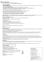
Table 5. Register Map Bank 0 Table: User Space

Name

Addr (0,Hex)

Access

Name

Addr (0,Hex)

Access

Name

Addr (0,Hex)

Access

Name

Addr (0,Hex)

Access

PRT0DR

00

RW

EP1_CNT0

40

#

80

C0

PRT0IE

01

RW

EP1_CNT1

41

RW

81

C1

02

EP2_CNT0

42

#

82

C2

03

EP2_CNT1

43

RW

83

C3

PRT1DR

04

RW

EP3_CNT0

44

#

84

C4

PRT1IE

05

RW

EP3_CNT1

45

RW

85

C5

06

EP4_CNT0

46

#

86

C6

07

EP4_CNT1

47

RW

87

C7

PRT2DR

08

RW

EP5_CNT0

48

#

88

I2C_XCFG

C8

RW

PRT2IE

09

RW

EP5_CNT1

49

RW

89

I2C_XSTAT

C9

R

0A

EP6_CNT0

4A

#

8A

I2C_ADDR

CA

RW

0B

EP6_CNT1

4B

RW

8B

I2C_BP

CB

R

PRT3DR

0C

RW

EP7_CNT0

4C

#

8C

I2C_CP

CC

R

PRT3IE

0D

RW

EP7_CNT1

4D

RW

8D

CPU_BP

CD

RW

0E

EP8_CNT0

4E

#

8E

CPU_CP

CE

R

0F

EP8_CNT1

4F

RW

8F

I2C_BUF

CF

RW

PRT4DR

10

RW

50

90

CUR_PP

D0

RW

PRT4IE

11

RW

51

91

STK_PP

D1

RW

12

52

92

D2

13

53

93

IDX_PP

D3

RW

14

54

94

MVR_PP

D4

RW

15

55

95

MVW_PP

D5

RW

16

56

96

I2C_CFG

D6

RW

17

57

97

I2C_SCR

D7

#

18

PMA0_DR

58

RW

98

I2C_DR

D8

RW

19

PMA1_DR

59

RW

99

D9

1A

PMA2_DR

5A

RW

9A

INT_CLR0

DA

RW

1B

PMA3_DR

5B

RW

9B

INT_CLR1

DB

RW

1C

PMA4_DR

5C

RW

9C

INT_CLR2

DC

RW

1D

PMA5_DR

5D

RW

9D

INT_CLR3 

DD

RW

1E

PMA6_DR

5E

RW

9E

INT_MSK2

DE

RW

1F

PMA7_DR

5F

RW

9F

INT_MSK1

DF

RW

20

60

A0

INT_MSK0

E0

RW

21

61

A1

INT_SW_EN

E1

RW

22

62

A2

INT_VC

E2

RC

23

63

A3

RES_WDT

E3

W

24

PMA8_DR

64

RW

A4

INT_MSK3

E4

RW

25

PMA9_DR

65

RW

A5

E5

26

PMA10_DR

66

RW

A6

E6

27

PMA11_DR

67

RW

A7

E7

28

PMA12_DR

68

RW

A8

E8

SPI_TXR

29

W

PMA13_DR

69

RW

A9

E9

SPI_RXR

2A

R

PMA14_DR

6A

RW

AA

EA

SPI_CR

2B

#

PMA15_DR

6B

RW

AB

EB

2C

TMP_DR0

6C

RW

AC

EC

2D

TMP_DR1

6D

RW

AD

ED

2E

TMP_DR2

6E

RW

AE

EE

2F

TMP_DR3

6F

RW

AF

EF

30

70

PT0_CFG

B0

RW

F0

USB_SOF0

31

R

71

PT0_DATA1

B1

RW

F1

USB_SOF1

32

R

72

PT0_DATA0

B2

RW

F2

USB_CR0

33

RW

73

PT1_CFG

B3

RW

F3

USBIO_CR0

34

#

74

PT1_DATA1

B4

RW

F4

USBIO_CR1

35

#

75

PT1_DATA0

B5

RW

F5

EP0_CR

36

#

76

PT2_CFG

B6

RW

F6

EP0_CNT0

37

#

77

PT2_DATA1

B7

RW

CPU_F

F7

RL

EP0_DR0

38

RW

78

PT2_DATA0

B8

RW

F8

EP0_DR1

39

RW

79

B9

F9

EP0_DR2

3A

RW

7A

BA

FA

EP0_DR3

3B

RW

7B

BB

FB

EP0_DR4

3C

RW

7C

BC

FC

EP0_DR5

3D

RW

7D

BD

FD

EP0_DR6

3E

RW

7E

BE

CPU_SCR1

FE

#

EP0_DR7

3F

RW

7F

BF

CPU_SCR0

FF

#

Gray fields are reserved; do not access these fields.      # Access is bit specific. 

[+] Feedback 

Содержание enCoRe V CY7C6431x

Страница 1: ...range is 19 to 50 kHz with a 32 kHz typical value Programmable Pin Configurations 25 mA sink current on all GPIO Pull Up High Z Open Drain CMOS drive modes on all GPIO Configurable inputs on all GPIO...

Страница 2: ...wires SPI communication over three or four wires runs at speeds of 46 9 kHz to 3 MHz lower for a slower system clock In I2 C slave mode the hardware address recognition feature reduces the already lo...

Страница 3: ...mlessly within the PSoC Designer interface and have been tested with a full range of debugging tools The choice is yours Assemblers The assemblers allow assembly code to be merged seamlessly with C co...

Страница 4: ...each other with valuator functions In the chip level view you perform the selection configuration and routing so that you have complete control over the use of all on chip resources Generate Verify a...

Страница 5: ...e h for example 14h or 3Ah Hexadecimal numbers may also be represented by a 0x prefix the C coding convention Binary numbers have an appended lowercase b for example 01010100b or 01000011b Numbers not...

Страница 6: ...ng ISSP pins that are not High Z at power on reset POR Table 1 16 Pin Part Pinout QFN Pin No Type Name Description 1 I O P2 3 Digital I O Crystal Input Xin 2 IOHR P1 7 Digital I O SPI SS I2C SCL 3 IOH...

Страница 7: ...Digital I O SPI CLK 8 IOHR P1 1 1 2 Digital I O ISSP CLK I2C SCL SPI MOSI 9 Power Vss Ground 10 I O D USB PHY 11 I O D USB PHY 12 Power Vdd Supply voltage 13 IOHR P1 0 1 2 Digital I O ISSP DATA I2C SD...

Страница 8: ...Description 1 NC NC No connection 2 I O P2 7 Digital I O 3 I O P2 5 Digital I O Crystal Out Xout 4 I O P2 3 Digital I O Crystal In Xin 5 I O P2 1 Digital I O 6 I O P4 3 Digital I O 7 I O P4 1 Digital...

Страница 9: ...I O P2 2 Digital I O 35 I O P2 4 Digital I O 36 I O P2 6 Digital I O 37 IOH P0 0 Digital I O 38 IOH P0 2 Digital I O 39 IOH P0 4 Digital I O 40 IOH P0 6 Digital I O 41 Power Vdd Supply voltage 42 NC...

Страница 10: ...e has a total register address space of 512 bytes The register space is also referred to as IO space and is broken into two parts Bank 0 user space and Bank 1 configu ration space The XIO bit in the F...

Страница 11: ...DR 5A RW 9A INT_CLR0 DA RW 1B PMA3_DR 5B RW 9B INT_CLR1 DB RW 1C PMA4_DR 5C RW 9C INT_CLR2 DC RW 1D PMA5_DR 5D RW 9D INT_CLR3 DD RW 1E PMA6_DR 5E RW 9E INT_MSK2 DE RW 1F PMA7_DR 5F RW 9F INT_MSK1 DF R...

Страница 12: ..._CR0 54 94 D4 15 EP2_CR0 55 95 D5 16 EP3_CR0 56 96 D6 17 EP4_CR0 57 97 D7 18 EP5_CR0 58 98 D8 19 EP6_CRO 59 99 D9 1A EP7_CR0 5A 9A DA 1B EP8_CR0 5B 9B DB 1C 5C 9C IO_CFG DC RW 1D 5D 9D OUT_P1 DD RW 1E...

Страница 13: ...ency Vdd Voltage 3 0V 3 MHz V a l i d O p e r a t i n g R e g i o n 5 5V 750 kHz 6 MHz 24 MHz IMO Frequency Vdd Voltage 3 MHz 3 0V SLIMO Mode 01 12 MHz SLIMO Mode 00 SLIMO Mode 10 Table 7 Units of Mea...

Страница 14: ...ock DC Accuracy DNL 1 2 LSb For any configuration INL 2 2 LSb For any configuration Offset Error 0 15 90 mV Operating Current 275 350 A Data Clock 2 25 12 MHz Source is chip s internal main oscil lato...

Страница 15: ...specific See Package Handling on page 25 The user must limit the power consumption to comply with this requirement Table 9 DC Chip Level Specifications Parameter Description Conditions Min Typ Max Un...

Страница 16: ...IOH 10 A Vdd 3 0V maximum of 10 mA source current in all I Os Vdd 0 2 V VOH2 High Output Voltage Port 0 2 or 3 Pins IOH 1 mA Vdd 3 0 maximum of 20 mA source current in all I Os Vdd 0 9 V VOH3 High Ou...

Страница 17: ...ysteresis Voltage 50 60 200 mV IIL Input Leakage Absolute Value 0 001 1 A CPIN Pin Capacitance Package and pin dependent Temp 25o C 0 5 1 7 5 pF Table 12 DC POR and LVD Specifications Symbol Descripti...

Страница 18: ...ing Programming or Verify 8 1 5 mA VOLV Output Low Voltage During Programming or Verify Vss 0 75 V VOHV Output High Voltage During Programming or Verify Vdd 0 9 Vdd V FlashENPB Flash Write Endurance 9...

Страница 19: ...jitter To next transition 3 5 3 5 ns Tudj2 Driver differential jitter To pair transition 4 0 4 0 ns Tfdeop Source jitter for differential transition To SE0 transition 2 5 ns Tfeopt Source SE0 interva...

Страница 20: ...AC GPIO Specifications Symbol Description Conditions Min Typ Max Units FGPIO GPIO Operating Frequency Normal Strong Mode Ports 0 1 0 12 MHz TRise23 Rise Time Strong Mode Ports 2 3 Vdd 3 3 to 5 5V 10...

Страница 21: ...ns TFSCLK Fall Time of SCLK 1 20 ns TSSCLK Data Setup Time to Falling Edge of SCLK 40 ns THSCLK Data Hold Time from Falling Edge of SCLK 40 ns FSCLK Frequency of SCLK 0 8 MHz TERASEB Flash Erase Time...

Страница 22: ...Repeated START Condition 4 7 0 6 s THDDATI2C Data Hold Time 0 0 s TSUDATI2C Data Setup Time 250 100 15 ns TSUSTOI2C Setup Time for STOP Condition 4 0 0 6 s TBUFI2C Bus Free Time Between a STOP and ST...

Страница 23: ...enCoRe V USB device along with the thermal impedances for each package Important Note Emulation tools may require a larger area on the target PCB than the chip s footprint For a detailed description...

Страница 24: ...CY7C6431x CY7C64345 CY7C6435x Document Number 001 12394 Rev G Page 24 of 28 Figure 10 32 Pin 5 x 5 x 0 55 mm QFN 001 42168 C Feedback...

Страница 25: ...ory A label on the package has details about the actual bake temperature and the minimum bake time to remove this moisture The maximum bake time is the aggregate time that the parts exposed to the bak...

Страница 26: ...C64316 16LKXCT 16 Pin QFN Tape and Reel 3x3 mm 32K 2K 11 Hi end FS USB dongle RC host module CY7C64343 32LQXC 32 Pin QFN 3x3 mm 8K 1K 25 Full speed USB mouse CY7C64343 32LQXCT 32 Pin QFN 3X3 mm 8K 1K...

Страница 27: ...ap tables Corrected a value in the DC Chip Level Specifications table C 1241024 TYJ ARI See ECN Corrected Idd values in Table 6 DC Chip Level Specifications D 1639963 AESA See ECN Post to www cypress...

Страница 28: ...e used only in conjunction with a Cypress integrated circuit as specified in the applicable agreement Any reproduction modification translation compilation or representation of this Source Code except...

Отзывы: