Copyright
©
2022
congatec
GmbH
TSTLm01
64/72
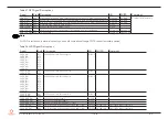
Table 29 SPI BIOS Flash Interface Signal Descriptions
Signal
Pin # Description
I/O
PU/PD
Comment
SPI_CS#
B97
Chip select for Carrier Board SPI BIOS Flash
O 3.3 VSB
Carrier shall pull to SPI_POWER when
external SPI is provided but not used
SPI_MISO
A92
Data in to module from carrier board SPI BIOS flash
I 3.3 VSB
SPI_MOSI
1
A95
Data out from module to carrier board SPI BIOS flash
O 3.3 VSB PU 4K75
3.3 VSB
SPI_MOSI is a bootstrap signal (see note
below)
SPI_CLK
A94
Clock from module to carrier board SPI BIOS flash
O 3.3 VSB
SPI_POWER
A91
Power source for carrier board SPI BIOS flash. SPI_POWER shall be used to power
SPI BIOS flash on the carrier only
+ 3.3 VSB
BIOS_DIS0#
A34
Selection strap to determine the BIOS boot device
I 3.3 VSB
PU 10 KΩ
3.3 VSB
Carrier shall be left as no-connect
BIOS_DIS1# B88
Selection strap to determine the BIOS boot device.
Refer to table 4.13 of the COM
Express Module Base Specification 3.0 for strapping options of BIOS disable signals
I 3.3 VSB
PU 10 KΩ
3.3 VSB
Carrier shall be left as no-connect
Note
1.
These signals have special functionality during the reset process. They may bootstrap some basic important functions of the module. For
more information refer to section 8.2 “Bootstrap Signals”.
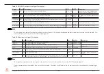
Table 30 Miscellaneous Signal Descriptions
Signal
Pin # Description
I/O
PU/PD
Comment
I2C_CK
B33
General purpose I²C port clock output/input
I/O 3.3 V PU 2K2 3.3 VSB
I2C_DAT
B34
General purpose I²C port data I/O line
I/O 3.3 V PU 2K2 3.3 VSB
SPKR
1
B32
Output for audio enunciator, the “speaker” in PC-AT systems
O 3.3 V
SPKR is a bootstrap signal (see
note below)
WDT
B27
Output indicating that a watchdog time-out event has occurred
O 3.3 V
PD 100 KΩ
FAN_PWMOUT
2
B101
Fan speed control. Uses the Pulse Width Modulation (PWM) technique to control
the fan’s RPM
O OD
3.3 V
FAN_TACHIN
2
B102
Fan tachometer input
I OD
PU 47K5 3.3 V
Requires a fan with a two pulse
output
TPM_PP
A96
Physical Presence pin of Trusted Platform Module (TPM). Active high. TPM chip has
an internal pull-down. This signal is used to indicate Physical Presence to the TPM
I 3.3 V
PD 1 KΩ
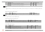
Note
1.
This signal has special function during the reset process. For more information, see section 9.2 “Bootstrap Signals”.
2.
Pins are protected on the module by a series schotty diode. Therefore, pull-down resistor is required on the carrier board for proper logic
level.


