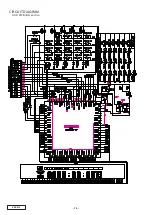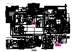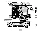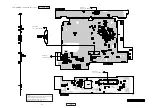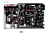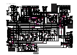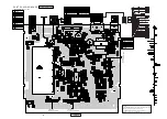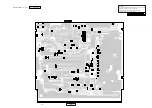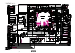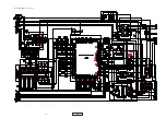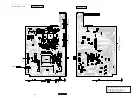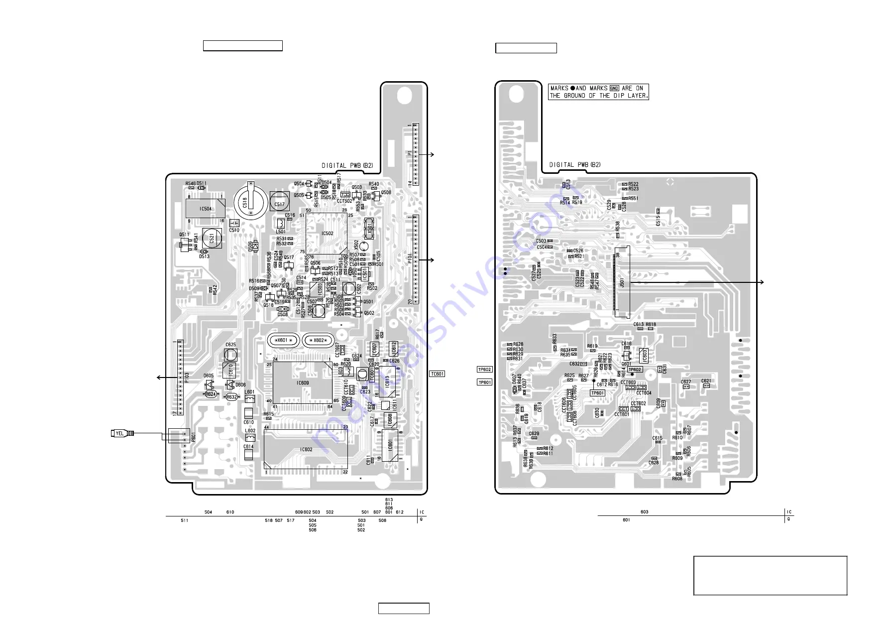
PRINTED WIRING BOARD
Digital PWB(B2) section
- 24 -
VRX630
to
P
A
G
E
1
7
F
LE
X
-P
W
B
/
J7
01
o
f L
C
D
P
W
B
-A
to
P
A
G
E
2
0
P
10
3
of
M
A
IN
P
W
B
VIDEO INPUT
to
P
A
G
E
2
0
P
1
of
M
A
IN
P
W
B
to
P
A
G
E
2
0
P
10
1
of
M
A
IN
P
W
B
COMPONENT SIDE
SOLDER SIDE
Caution:
COMPONENT SIDE: Parts on the component side seen
from the component side are indicated.
SOLDER SIDE: Parts on the solder side seen
from the solder side are indicated.
GND
VIDEO
Содержание pro audio vrx 630
Страница 14: ...DCP PWB B4 section 14 VRX630 CIRCUIT DIAGRAM ...
Страница 15: ...LCD PWB B3 section 15 VRX630 ...
Страница 18: ...Main PWB B1 section 1 2 18 VRX630 CIRCUIT DIAGRAM ...
Страница 22: ...Digital PWB B2 section 1 2 22 VRX630 CIRCUIT DIAGRAM ...
Страница 23: ...Digital PWB B2 section 2 2 23 VRX630 ...

