background image

- 2 -

VRX630

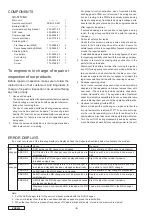
COMPONENTS

QC-6710B-A

Main unit

-----------

1

Remote control unit

RCB-130-601

1

Battery(SUM-3)

-----------

2

Universal mounting bracket

300-9677-00

1

DCP case

335-6035-41

1

Power supply lead

854-6356-51

1

Outer escutcheon

940-7715-04

1

Parts bag(No.1)

-----------

Flat head screw(M5x8)

714-5008-41

4

Sems hexagonal bolt(M5x8)

716-0496-01

5

Parts bag(No.2)

-----------

Hook plate

331-0488-20

2

Cord clamp

335-0833-07

1

Spacer

345-3653-20

1

Screw

716-0726-01

1

To engineers in charge of repair or

inspection of our products.

Before repair or inspection, make sure to follow the

instructions so that customers and Engineers in

charge of repair or inspection can avoid suffering

any risk or injury.

1. Use specified parts.

The system uses parts with special safety features against

fire and voltage. Use only parts with equivalent character-

istics when replacing them.

The use of unspecified parts shall be regarded as remod-

eling for which we shall not be liable. The onus of product

liability (PL) shall not be our responsibility in cases where

an accident or failure is as a result of unspecified parts

being used.

2. Place the parts and wiring back in their original positions

after replacement or re-wiring.

For proper circuit construction, use of insulation tubes,

bonding,gaps to PWB, etc, is involved. The wiring connec-

tion and routing to the PWB are specially planned using

clamps to keep away from heated and high voltage parts.

Ensure that they are placed back in their original positions

after repair or inspection.

If extended damage is caused due to negligence during

repair, the legal responsibility shall be with the repairing

company.

3. Check for safety after repair.

Check that the screws, parts and wires are put back se-

curely in their original position after repair. Ensure for

safety reasons there is no possibility of secondary ploblems

around the repaired spots.

If extended damage is caused due to negligence of repair,

the legal responsibility shall be with the repairing company.

4. Caution in removal and making wiring connection to the

parts for the automobile.

Disconnect the battery terminal after turning the ignition

key off. If wrong wiring connections are made with the bat-

tery connected, a short circuit and/or fire may occur. If ex-

tensive damage is caused due to negligence of repair, the

legal responsibility shall be with the repairing company.

5. Cautions regarding chips.

Do not reuse removed chips even when no abnormality is

observed in their appearance. Always replace them with

new ones. (The chip parts include resistors, capacitors,

diodes, transistors, etc). The negative pole of tantalum

capacitors is highly susceptible to heat, so use special care

when replacing them and check the operation afterwards.

6. Cautions in handling flexible PWB

Before working with a soldering iron, make sure that the

iron tip temperature is around 270 . Take care not to ap-

ply the iron tip repeatedly(more than three times)to the

same patterns. Also take care not to apply the tip with force.

7. Turn the unit OFF during disassembly and parts replace-

ment. Recheck all work before you apply power to the unit.

ERROR DISPLAYS

If an error occurs,one of the following displays is displayed.Take the measures described below to eliminate the problem.

CD

changer

MD

changer

Error display

ERROR 2

ERROR 3

ERROR 6

ERROR H

EEROR 2

ERROR 3

ERROR 6

Cause

A CD inside the CD changer is not loaded.

A CD inside the CD changer cannot be played due to

scratches,etc.

A CD inside the CD changer cannot be played because it

is loaded upside-down.

Displayed when the temperature in the MD changer is

too high and playback has been stopped automatically.

An MD inside the MD changer is not loaded.

An MD inside the MD changer cannot be played due to

scratches,etc.

A MD inside the MD changer cannot be played because

it is loaded upside-down.

Displayed when a non-recorded MD is loaded in the MD

changer.

Measure

This is a failure of CD changer's mechanism.

Replace with a non-scratched,non-warped

disc.

Eject the disc then reload it properly.

Lower the surrounding temperature and wait

for a while to cool off MD changer.

This is a failure of MD changer's mechanism.

Replace with a non-scratched,non-warped

disc.

Eject the disc then reload it properly.

Load a pre-recorded MD in the MD changer.

Note:

1. For the DVD changer,refer to the service manual provided with the DVD changer.

2. If an error display other than the ones described above appears, press the reset button.

3. When the reset button is pressed,frequencies of TV/radio stations,titles,etc. stored in the memory are cleared.

Содержание pro audio vrx 630

Страница 1: ...ut min 200mVrms LCD monitor section Screen size 6 5 inch wide type 142mm Width x 78mm Height Display method Transmission type TN Liquid Crystal Display Drive method TFT thin film transistor active matrix driving Pixels 280 800 1200 x 234 General Power supply voltage 14 4V DC 10 8 to 15 6V allowable Ground Negative Current consumption 4 0A 1W Auto antenna rated current 500mA less Dimensions mm Main...

Страница 2: ...onnected a short circuit and or fire may occur If ex tensive damage is caused due to negligence of repair the legal responsibility shall be with the repairing company 5 Cautions regarding chips Do not reuse removed chips even when no abnormality is observed in their appearance Always replace them with new ones The chip parts include resistors capacitors diodes transistors etc The negative pole of ...

Страница 3: ...n NTSC mode Make sure the voltage of TP706 is 1 88 0 1 0 1V 2 RGB AMP CONT G adjustment NTSC mode Adjust VR707 RBG AMP so that VBB voltage of TP710 is 4 0 0 5 0 5V Adjust VR703 CONT so that VBW voltage of TP710 is 3 8 0 05 0 05V 3 BRT R Adjustment NTSC mode Adjust VR705 BRT R so that VBB voltage of TP711 is 4 0 0 05 0 05V 4 BRT B Adjustment NTSC mode Adjust VR706 BRT B so that VBB voltage of TP709...

Страница 4: ...STNBY_ O H Amplifier ON pin 80 NU O Not in use pin 81 PHON INT IN Telephone interrupt signal input pin 82 NU IN Not in use pin 83 NU IN Not in use pin 84 FM SD IN FM SD input pin 85 AM SD IN AM SD input pin 86 NU IN Not in use pin 87 NU O Not in use pin 88 NU O Not in use pin 89 NU IN Not in use pin 90 NU IN Not in use pin 91 NU IN Not in use pin 92 NU IN Not in use pin 93 SD SPEED O Station detec...

Страница 5: ...IC104 MIX FM AM FM AM TUNER BL1 IF REQ FM AM ST AM SD FM SD DI DO CLK CE 10MHz N _P CS SCLK SIN CRYSTAL NTSC 14 3M PAL 17 7M IC603 IC609 B OSDC IC602 8M ROM RESET SW TILT SW POWER SW OPEN CLOSE SW DCP section ILL KEY INPUT IC901 DCP CONT DCP CLK DCP DATA KEY REQ DCP CE EXIT STBY IC701 EX I O NTSC PAL SW ACC 5V B U 5V MEMO 5V ACC ON IC502 SYSTEM CONTROL ILL PKB TEL ACC VIDEO MOT ON AV ON ACC ON FL ...

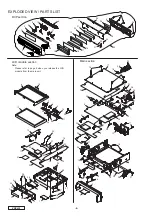
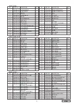
Страница 6: ...20 14 23 21 23 30 18 11 31 32 15 27 27 16 26 17 27 25 5 25 4 24 33 2 1 1 3 24 11 18 18 16 13 34 23 31 19 21 20 33 32 22 10 17 9 35 8 30 7 6 29 12 28 27 26 15 16 5 27 26 25 15 24 4 14 3 14 2 1 22 26 EXPLODED VIEW PARTS LIST DCP section LCD module section Note Please refer to page 8 when you release the LCD module from the main unit Main section ...

Страница 7: ...7 2613 02 DIAL SUPPORT 1 16 335 5161 00 LOCK 2 17 335 6089 00 CONNECT COVER 1 18 039 1521 00 FLEXIBLE PWB 1 19 378 0515 00 BADGE Clarion 1 20 816 2439 50 FLAT WIRE 1 21 347 6110 00 INSULATOR 1 22 331 2789 00 SHIELD CASE 1 23 702 2605 80 TAP SCREW 2 6x5 4 24 716 0872 02 PAD SCREW 6 25 702 2606 87 TAP SCREW 2 6x6 4 26 702 2006 89 TAP SCREW 2 6x6 2 27 702 2010 87 TAP SCREW M2x10 5 28 345 8378 00 SPAC...

Страница 8: ...hooks of the Flexible PWB cover No 1 from the LCD module and the slide mechanism assembly No 5 6 Remove the flexible PWB cover No 1 and the IT screws No 14x4 Fig 3 Slide motor Flexible PWB EXPLODED VIEW PARTS LIST Slide mechanism section 948 0530 20 3 2 1 Slide plate assembly Slide plate assembly 4 Slide plate sub assembly 4 Slide plate sub assembly Gear plate assembly Gear plate assembly 5 6 Note...

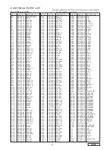
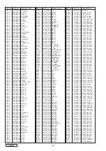
Страница 9: ...180 042 0595 62 16V10uF C181 184 2283 32 16V2200uF C182 166 2201 50 22pF CH C183 172 1041 11 0 1uF C184 042 0595 62 16V10uF C186 042 0592 58 16V10uF C187 042 0592 58 16V10uF C188 042 0592 58 16V10uF C189 166 2201 50 22pF CH C190 042 0595 62 16V10uF C191 042 0592 58 16V10uF C192 168 1032 55 0 01uF C193 042 0595 62 16V10uF C194 168 1032 55 0 01uF C195 042 0592 58 16V10uF C196 042 0592 58 16V10uF C19...

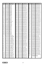
Страница 10: ...31 15 1 16W 22k ohm R149 119 3311 15 1 16W 330 ohm R150 119 1031 15 1 16W 10k ohm R151 119 2231 15 1 16W 22k ohm R154 119 6831 15 1 16W 68k ohm R155 119 1031 15 1 16W 10k ohm R156 119 2221 15 1 16W 2 2k ohm R157 119 2721 15 1 16W 2 7k ohm R158 119 4731 15 1 16W 47k ohm R159 119 2231 15 1 16W 22k ohm R160 119 2231 15 1 16W 22k ohm R161 119 2231 15 1 16W 22k ohm R162 119 2231 15 1 16W 22k ohm R163 1...

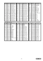
Страница 11: ...4 93 RN1403 R501 119 1031 15 1 16W 10k ohm R502 119 1231 15 1 16W 12k ohm R503 119 4721 15 1 16W 4 7k ohm R504 119 4721 15 1 16W 4 7k ohm R505 119 4741 15 1 16W 470k ohm R506 119 4741 15 1 16W 470k ohm R507 119 1021 15 1 16W 1k ohm R508 119 1021 15 1 16W 1k ohm R509 119 1011 15 1 16W 100 ohm R510 119 5621 15 1 16W 5 6k ohm R511 119 1021 15 1 16W 1k ohm R512 119 4721 15 1 16W 4 7k ohm R513 119 4731...

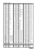
Страница 12: ... L708 010 2199 83 56uH J L709 010 4013 00 23 9uH L710 010 2199 80 33uH J LCD2 379 1162 41 DISPLAY P701 076 0529 02 2P P702 076 0624 80 30P Q701 190 1213 00 2SA1213 Q702 125 2004 92 RN1402 Q703 125 2036 90 FB1J3P Q704 192 2873 00 2SC2873 Q705 190 1738 00 2SA1738 Q706 125 0002 93 RN2403 Q707 125 2004 92 RN1402 Q708 125 2004 92 RN1402 Q709 125 2004 92 RN1402 Q710 125 2004 93 RN1403 Q711 125 0002 92 R...

Страница 13: ...2 6009 58 33k ohm VR707 012 6009 58 33k ohm VR708 012 6009 52 1k ohm X701 061 1078 00 3 5795MHz X702 061 3036 00 4 433619MHz REF No PART No DESCRIPTION REF No PART No DESCRIPTION REF No PART No DESCRIPTION REF No PART No DESCRIPTION REF No PART No DESCRIPTION REF No PART No DESCRIPTION DCP PWB section B4 C901 178 1055 79 1uF C902 178 1055 79 1uF D901 001 7064 90 CL 170SR D902 001 7064 90 CL 170SR ...

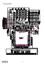
Страница 14: ...DCP PWB B4 section 14 VRX630 CIRCUIT DIAGRAM ...

Страница 15: ...LCD PWB B3 section 15 VRX630 ...

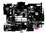
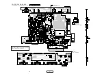
Страница 16: ...1 of LCD PWB A 1 12 13 24 25 36 37 48 to PAGE 17 J901 of DCP PWB to PAGE 17 J901 of LCD PWB B Caution COMPONENT SIDE Parts on the component side seen from the component side are indicated SOLDER SIDE Parts on the solder side seen from the solder side are indicated COMPONENT SIDE ...

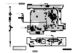
Страница 17: ...PWB to PAGE 16 P702 of LCD PWB A to PAGE 16 6 5 INDICATOR to PAGE 16 J703 of LCD PWB A Caution COMPONENT SIDE Parts on the component side seen from the component side are indicated SOLDER SIDE Parts on the solder side seen from the solder side are indicated SOLDER SIDE ...

Страница 18: ...Main PWB B1 section 1 2 18 VRX630 CIRCUIT DIAGRAM ...

Страница 19: ...LEFT SP H REAR RIGHT SP I BACK UP J ACC K ILLUMINATION L PARKING BRAKE M PHONE INT N REMOTE TURN ON O NC P REAR RIGHT SP 1 SEL3 2 SEL2 3 REMOTE CONTROL 4 VIDEO IN 5 AUDIO R IN 6 AUDIO L IN 7 GND 8 S GND 1 GND 2 BACK UP 3 BUS L ch 4 NC 5 NC 6 BUS 7 BUS R ch 8 BUS R ch 9 SYS ACC 10 BUS 11 BUS L ch 12 ILLUMINATION 13 NC C127 3300p ...

Страница 20: ...IN 5 AUDIO R IN 6 AUDIO L IN 7 GND 8 S GND Ce NET VISUAL CCD A GND B FRONT LEFT SP C FRONT LEFT SP D FRONT RIGHT SP E FRONT RIGHT SP F REAR LEFT SP G REAR LEFT SP H REAR RIGHT SP I BACK UP J ACC K ILLUMINATION L PARKING BRAKE M PHONE INT N REMOTE TURN ON O NC P REAR RIGHT SP Caution COMPONENT SIDE Parts on the component side seen from the component side are indicated SOLDER SIDE Parts on the solde...

Страница 21: ...PWB B1 section 21 VRX630 Caution COMPONENT SIDE Parts on the component side seen from the component side are indicated SOLDER SIDE Parts on the solder side seen from the solder side are indicated SOLDER SIDE ...

Страница 22: ...Digital PWB B2 section 1 2 22 VRX630 CIRCUIT DIAGRAM ...

Страница 23: ...Digital PWB B2 section 2 2 23 VRX630 ...

Страница 24: ...AGE 20 P103 of MAIN PWB VIDEO INPUT to PAGE 20 P1 of MAIN PWB to PAGE 20 P101 of MAIN PWB COMPONENT SIDE SOLDER SIDE Caution COMPONENT SIDE Parts on the component side seen from the component side are indicated SOLDER SIDE Parts on the solder side seen from the solder side are indicated GND VIDEO ...

Отзывы: