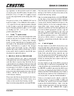
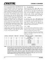
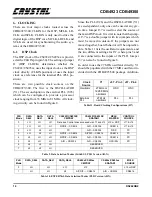
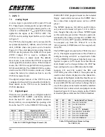
background image

Preliminary Product Information

This document contains information for a new product.
Cirrus Logic reserves the right to modify this product without notice.

1

Copyright 

 Cirrus Logic, Inc. 2000

(All Rights Reserved)

P.O. Box 17847, Austin, Texas 78760
(512) 445 7222   FAX: (512) 445 7581
http://www.cirrus.com

CDB4923

CDB49300

Evaluation Board for CS4923/CS49300 Families

Features

l

CDB4923 demonstrates 5.1 channel decode 
capability of the CS4923 family

l

CDB49300 demonstrates 5.1 channel 
decode capability of CS49300 family

l

6 discrete analog outputs driven by CS4340 
DACs

l

4 S/PDIF optical outputs 

l

Accepts analog input, S/PDIF digital input, 
Bursty compressed data 

l

Discrete PLL which can provide multiple 
sampling frequencies 

l

Interfaces to a personal computer through 
the parallel port

l

Stake headers provide convenient location 
for direct wiring to control signals from off-
board microcontroller 

l

Interface for external memory card

l

Digital and analog patch areas

Description

The CDB4923 and CDB49300 customer development
boards provide the means to fully evaluate the
CS4923/4/5/6/7/8 and CS49300 family of audio decod-
ers. Compressed data can be delivered in IEC61937
format via the S/PDIF port and in bursty mode via the PC
interface. PCM data can be accepted through the digital
input connectors or from the on-board ADC. Six chan-
nels of audio are provided on the six analog outputs and
on three optical S/PDIF transmitters. CLKIN for the DSP
can be derived either from the on-board oscillator or the
external PLL. MCLK can be extracted from incoming
S/PDIF streams, generated with the external PLL, or
mastered by the audio decoder.

The CDB4923/300 incorporates a Crystal Multichannel
Audio Decoder, the CS4340 24-Bit Audio D/A Converter,
the CS8414 Digital Audio Interface Receiver, the
CS8404A Digital Audio Interface Transmitter, and the
CS5334 20-Bit Stereo A/D Converter. 

ORDERING INFORMATION

CDB4923

Evaluation Board

CDB49300

Evaluation Board

I

Analog
Output

Stereo
Analog In

Digital Output

Digital Input

Control

Interface

Patch Area

RESET

CS

8414

PL

L

+3.3V

+2.5V

CS492x
CS493xx

OSC

PLD

CS8404A

CS8404A

CS8404A

CS4340

CS4340

CS4340

CS5334

DIGITAL SOUND

P R O C E S S I N G

C R Y S T A L

®

JAN ‘00

DS262DB2

Содержание CS492 Series

Страница 1: ...9300 customer development boards provide the means to fully evaluate the CS4923 4 5 6 7 8 and CS49300 family of audio decod ers Compressed data can be delivered in IEC61937 format via the S PDIF port and in bursty mode via the PC interface PCM data can be accepted through the digital input connectors or from the on board ADC Six chan nels of audio are provided on the six analog outputs and on thre...

Страница 2: ...sure that the information contained in this document is accurate and reliable However the information is subject to change without notice and is provided AS IS without warranty of any kind express or implied No responsibility is assumed by Cirrus Logic Inc for the use of this information nor for infringements of patents or other rights of third parties This document is the property of Cirrus Logic...

Страница 3: ...D BY NUMBER 46 16 APPENDIX J SWITCH SUMMARY 47 LIST OF FIGURES Figure 1 External Memory Example 9 Figure 2 CDB4923 300 Data Paths 11 Figure 3 Audio Clocking 12 Figure 4 Audio Clocking 12 Figure 4 CS492x CS493xx 18 Figure 5 System Power 19 Figure 6 PC Interface 20 Figure 7 Control Logic 21 Figure 8 Clocking 22 Figure 9 Analog Input 23 Figure 10 Digital Input 24 Figure 11 D A Converters 25 Figure 12...

Страница 4: ... Modes PLD Version AB X 14 Table 11 Board Clocking Configurations J37 14 Table 12 PCLK Configurations 15 Table 13 Audio Frequency Selection J58 15 Table 14 CS5334 Digital Output Formats S4 16 Table 15 Digital Output Format settings for CS8414 S1 16 Table 16 CS4340 Digital Input Formats S4 17 Table 17 Digital Input Format settings for CS8404A S2 17 Table 18 CS492x CS493xx Host Interface Mode Select...

Страница 5: ... filter components for the CDB4923 are R246 0 Ω C155 0 22 µF The relevant PLL filter components for the CDB49300 are R246 33 kΩ C155 0 22 µF C113 0 01 µF Although the boards are tailored for one specific family of audio decoders the operation of the CDB4923 and CDB49300 is effectively the same This document will generically refer to the CDB4923 300 except in those instances where there is a differ...

Страница 6: ...ed with the board When properly configured the external PLL can provide a processor clock frequency ranging from 33 MHz to 81 MHz When the external PLL is used for the DSP processor clock it can also be used to master the system oversampling clock MCLK The CDB4923 300 features six channels of analog output provided by three CS4340 DACs The out puts are provide a 3 5 Vpp signal and each output has ...

Страница 7: ...ews cs4923 html This document and all other documentation per taining to the CS493xx family of decoders can be found at the following website http www cirrus com products overviews cs49300 html As the focus of the board the CS492x CS493xx performs all processing of digital audio The DSP section of the board is illustrated in Figure 4 The CS492x CS493xx can be fed compressed data or linear PCM from...

Страница 8: ...boot The CS493xx also has a static RAM interface The CDB49300 MEM external memory board is tai lored for the CDB49300 The CDB49300 MEM schematic can be found in Figure 21 The CDB4923 300 has been designed to interface to both the CRD4923 MEM and CDB49300 MEM daughter boards The card plugs directly on to J11 oriented such that the CS492x CS493xx is not cov ered as shown in Figure 1 Please consult t...

Страница 9: ... Data Selection All PLD modes are selected using DIP switch S3 The PLD U11 and switch S3 are shown in Figure 7 A specialized IC U12 the MAX708 has been in cluded on the CDB4923 300 in order to generate a system reset at power up when the digital power begins to fail and when the system reset button SW1 is depressed This chip helps to insure con sistent operation on the board by providing a 200 ms ...

Страница 10: ...DB4923 300 is accomplished using the parallel port J29 A floppy disk is included with the CDB4923 300 which contains the control software described in Appendix F Board Control Software 5 1 2 Data All of the Data Selection Modes shown in Table 3 imply PC control In Table 4 a brief description is given for each data source listed in Table 3 The general data flow of the system is illustrated in Figur...

Страница 11: ...414 The CS8414 U13 delivers the payload from an IEC60958 linear PCM or IEC61937 nonlinear PCM encoded bit stream The incoming S PDIF stream is connected to either J32 or J30 A D CS5334 The CS5334 U25 delivers stereo PCM which has been encoded from the analog input signals on J55 and J56 PC A compressed digital audio stream is delivered in bursty format to the parallel port of the CS492x CS493xx fr...

Страница 12: ...led with the demo board will not be functional The main DSP clock is always provided by the CDB4923 300 please see the Clocking section to determine how to select the oscillator or external PLL and the output signals AUDATA0 2 are still routed to the CS8404A S PDIF transmitters and CS4340 DACs Depending on the EXTERNAL mode selected the user may be responsible for all data control and clock signal...

Страница 13: ...s J13 J20 and the digital outputs J45 J47 The analog outputs J13 J20 can be found in Figure 12 and the digital outputs can be found in Figure 13 The information in Table 9 summarizes the opera tion of switch S3 The table shows the data routing configuration the MCLK source and the method of board control This is intended as a quick refer ence and can also be found in Appendix J Switch Summary Pin ...

Страница 14: ...on If the jumpers are not moved together board behavior will be unpredict able Table 11 lists the oscillator requirements and the two different settings for J37 where pins 3 and 4 are connected to the inputs of the PLD Jumper J37 can also be found in Figure 8 In order to use the 27 MHz oscillator directly Y1 should be populated with the 27 MHz oscillator in cluded with the CDB4923 300 package Addi...

Страница 15: ...the CDB4923 300 can come from four different sources when using a PROVID ED mode Some PLD modes use the MCLK gener ated by the CS8414 S PDIF receiver U13 when there is an incoming S PDIF stream In PLD mode 2 the DSP generates MCLK when it is decoding a compressed bit stream delivered by the PC Some modes can select between an MCLK which is sim ply the frequency of the on board oscillator Y1 or a p...

Страница 16: ... The S PDIF inputs are J30 RCA and J32 Opti cal and can be found in Figure 10 It is vital to note though that only one of these S PDIF inputs can be used at any given time The active jack is de termined by the setting of jumper J31 S PDIF IN When J31 is in the OPT position S PDIF data will be accepted only from J32 When J31 is in the RCA position S PDIF data will be accepted only from J30 The S PD...

Страница 17: ...sent on analog outputs J13 J16 J18 and J20 can also be found on the digital outputs J45 J47 AOUTDIG0 AOUTDIG2 The optical transmitters are driven by CS8404A S PDIF trans mitters U19 21 The CS8404As are configured to operate in consumer mode by default The mode of operation and status bits can be controlled by in stalling a 16 pin header in J44 and placing jumpers on the signals that are to be prog...

Страница 18: ...CDB4923 CDB49300 18 DS262DB2 9 APPENDIX A SCHEMATICS Figure 4 CS492x CS493xx ...

Страница 19: ...CDB4923 CDB49300 DS262DB2 19 Figure 5 System Power ...

Страница 20: ...CDB4923 CDB49300 20 DS262DB2 Figure 6 PC Interface ...

Страница 21: ...CDB4923 CDB49300 DS262DB2 21 Figure 7 Control Logic ...

Страница 22: ...CDB4923 CDB49300 22 DS262DB2 Figure 8 Clocking ...

Страница 23: ...CDB4923 CDB49300 DS262DB2 23 Figure 9 Analog Input ...

Страница 24: ...CDB4923 CDB49300 24 DS262DB2 Figure 10 Digital Input ...

Страница 25: ...CDB4923 CDB49300 DS262DB2 25 Figure 11 D A Converters ...

Страница 26: ...CDB4923 CDB49300 26 DS262DB2 Figure 12 Analog Output ...

Страница 27: ...CDB4923 CDB49300 DS262DB2 27 Figure 13 Digital Output ...

Страница 28: ...CDB4923 CDB49300 28 DS262DB2 Figure 14 Top Layer ...

Страница 29: ...CDB4923 CDB49300 DS262DB2 29 Figure 15 Bottom Layer ...

Страница 30: ...CDB4923 CDB49300 30 DS262DB2 Figure 16 SSTOP ...

Страница 31: ...CDB4923 CDB49300 DS262DB2 31 Figure 17 ASYSTOP ...

Страница 32: ...CDB4923 CDB49300 32 DS262DB2 Figure 18 Layer 2 ...

Страница 33: ...CDB4923 CDB49300 DS262DB2 33 Figure 19 Layer 3 ...

Страница 34: ...X7R 1206 50V 10 11 1 C113 1206CG471J9BB2 PHILIPS CAP 470PF COG 1206 50V 5 12 3 C119 C122 C134 T491C106K020AS KEMET CAP 10UF TANT 6032 20V 10 13 2 C128 C120 C1206C100J5GAC KEMET CAP 10PF COG 1206 50V 5 14 2 C131 C121 C1206C222J5GAC KEMET CAP 2200PF COG 1206 50V 5 15 2 C140 C142 C1206C470J5GAC KEMET CAP 47PF COG 1206 50V 5 16 1 C154 C340C225K5R5CA KEMET CAP 2 2UF X7R C340 50V 10 17 1 C155 C330C103K5...

Страница 35: ... 1 R87 R88 R89 R90 R91 R92 R94 R96 R98 R 100 R102 R103 R104 R105 R106 R107 R110 R126 R129 R130 R131 R190 R191 R198 R20 0 R239 R240 R241 CRCW1206330JT DALE RES 33 OHM 1206 5 1 4W METAL FILM 45 6 R50 R55 R60 R67 R75 R81 CRCW12065610FT DALE RES 560 OHM 1206 1 1 4W METAL FILM 46 3 R84 R85 R226 CRCW12061001FT DALE RES 1K OHM 1206 1 1 8W METAL FILM 47 5 R86 R210 R217 R220 R229 CRCW1206151JT DALE RES 150...

Страница 36: ...CUIT 24 bit 96kHz DAC 16pin SOIC 72 3 U19 U20 U21 CS8404A CS CRYSTAL SEMICONDUCTOR INTEGRATED CIRCUIT SOIC24 WIDE 73 2 U23 U24 MC33078 P MOTOROLA INTEGRATED CIRCUIT DUAL OP AMP DIP 8 74 2 UX23 UX24 110 93 308 41 001 MILL MAX S0CKET 300 MILL DIP 8 75 1 U25 CS5334 KS CRYSTAL SEMICONDUCTOR INTEGRATED CIRCUIT SSOP20 76 1 U26 MK2744 10S MICRO CLOCK INTEGRATED CIRCUIT 77 1 U27 LM2937ET 2 5 NATIONAL SEMI...

Страница 37: ... A12 4 A11 25 A10 23 A09 26 A08 27 O 0 13 O 1 14 O 2 15 O 3 17 O 4 18 O 5 19 O 6 20 O 7 21 CE 22 O E 24 P G M 31 VPP 1 V C C 32 G N D 16 P 1 1 2 3 4 5 6 7 8 9 10 11 12 13 14 15 16 17 18 19 20 U 5 A 74LVC125 2 3 1 U 5 B 74LVC125 5 6 4 U 5 C 74LVC125 9 8 10 U 5 D 74LVC125 12 11 13 U 5 E 74LVC125 7 14 R 1 10k R 1 4 10k R 1 3 10k U 2 TC74VHC574FW Q 7 12 Q 6 13 Q 5 14 Q 4 15 Q 3 16 Q 2 17 Q 1 18 Q 0 19...

Страница 38: ...7 49 9 R18 49 9 U5 CY7C109V33 19 20 21 22 23 24 25 26 9 10 11 12 13 14 15 16 17 18 7 6 5 4 3 2 1 32 31 30 29 28 8 27 A1 A0 D0 D1 D2 GND D3 D4 NC A16 A14 A12 A7 A6 A5 A4 A3 A2 A15 CE2 WE A13 A8 A9 A11 OE A10 CE1 D7 D6 VCC D5 R15 49 9 R14 49 9 R11 49 9 C7 0 1uF R10 49 9 U3 74LVC574 12 13 14 15 16 17 18 19 11 2 3 4 5 6 7 8 9 10 1 20 Q7 Q6 Q5 Q4 Q3 Q2 Q1 Q0 CK D0 D1 D2 D3 D4 D5 D6 D7 GND OE VCC C6 47u...

Страница 39: ...cation mode used by the CS492x CS493xx If the DSP is using a communication mode which does not match the software setting results will be unpredictable Please see Digital Signal Processor of this datasheet to learn how to change the DSP s com munication mode The source code for all programs can be found on the floppy disk provided with the CDB4923 300 These programs are documented and will provide...

Страница 40: ...Y mode designator i I2C s SPI m MOT n INT v disable verbose mode h this message default CDB30RST program used to perform hard reset or soft reset on the CS492x CS493xx Usage cdb30rst s pXXX mY v h s Soft Reset p parallel port address XXX address 0x278 378 or 3bc m communication mode Y mode designator i I2C s SPI m MOT n INT v disable verbose mode h this message default PARLLPLY program used to del...

Страница 41: ... been detected The user should specify invalid for any application code or configuration file which does not exist This program only allows serial control Usage cdb30_ad AC3 ld AC3 cfg MPEG ld MPEG cfg DTS ld DTS cfg PCM ld PCM cfg pXXX mY v Specify invalid for non existent ld cfg p parallel port address XXX address 0x278 378 or 3bc m communication mode Y mode designator i I2C s SPI v disable verb...

Страница 42: ... 5 DSP U1 CS492x CS493xx Multi Channel Audio Decoder Figure 4 13 6 INPUT U9 Signal Buffer for Parallel Port Figure 6 U10 Signal Buffer for Parallel Port Figure 6 U13 CS8414 S PDIF receiver Figure 10 U23 MC33078 Analog Input Buffer Figure 9 U24 MC33078 Analog Input Buffer Figure 9 U25 CS5334 20 bit A D converter Figure 9 13 7 OUTPUT U16 CS4340 20 bit D A converter Figure 11 U17 CS4340 20 bit D A co...

Страница 43: ...in the outgoing S PDIF stream created by the CS8404A More details can be found in the datasheet for the CS8404A and the specifications for IEC60958 and IEC61937 bitstreams Default All bits HI Not Populated 14 3 DSP JUMPERS J1 This jumper is used to control the internal clocking of the CS492x CS493xx When in the CLKIN position the CS492x CS493xx uses the clock on the CLKIN pin to drive the DSP core...

Страница 44: ...INSTALLED J60 This jumper connects DSP_PWR to the digital side of the CS492x CS493xx Digital current consumption can be measured by removing this jumper and connecting an ammeter in series with the jumper Default INSTALLED J63 This jumper is used to select the maximum voltage at which the I O pins of the system PLD U11 will drive its outputs The user can select between 3 3 V and 2 5 V Default 3 3 ...

Страница 45: ...t LO J68 Jumper used to set the values of the PS0 pin of U26 This jumper in conjunction with J67 and J72 determines the processor clock frequency provided by the external PLL Please refer to Table 12 or Table 22 for more details Default HI J70 Jumper used to set the values of the AS1 pin of U26 This jumper in conjunction with J71 de termines the MCLK frequency provided by the external PLL Please r...

Страница 46: ...nnel Status Bits Audio Output Jumpers Default All bits HI Not Populated J52 MASTER SLAVE clocking mode of the CS5334 Audio Input Jumpers Default SLAVE J59 CS492x CS493xx Analog Power Power Jumpers Default INSTALLED J60 CS492x CS493xx Digital Power Power Jumpers Default INSTALLED J62 CS492x CS493xx PSEL pin DSP Jumpers Default HI J63 PLD I O Power Selection Power Jumpers Default 3 3 V J65 CS8414 SE...

Страница 47: ...ailable digital input format Table 22 shows all available PLL settings for the external PLL on the CDB4923 4930 Table 24 lists all possible data routing possibilities and the associated MCLK source for the CDB4923 300 RD J3 WR J2 PSEL J62 Host Interface Mode 0 1 1 Serial I2 C PSEL SCDIO 1 0 X Serial SPI 1 1 0 8 bit Intel 1 1 1 8 bit Motorola Table 18 CS492x CS493xx Host Interface Mode Selection 34...

Страница 48: ... HI HI LO LSB Justified 18 Bits HI HI HI MSB Last 16 24 Bits Table 23 Digital Input Format settings for CS8404A S2 PLD Mode DATA SEL2 DATA SEL1 DATA SEL0 CS492X CS493XX CMPDAT CS492X CS493XX SDATAN1 MCLK MASTER CONTROL SOURCE 0 LO LO LO Data and Control lines accessed via J11 and J12 J12 or DSP J11 J12 1 LO LO HI S PDIF CS8414 A D CS5334 CS8414 J11 J12 2 LO HI LO PC A D CS5334 DSP PC 3 LO HI HI S ...

Страница 49: ... Notes ...

Страница 50: ......

Отзывы: