


Lepton
9
- Technical Information Manual
18
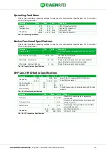
Parameter
Min.
Typ.
Max.
Unit
Conditions
ADC (Pin 13)
Resolution
12
Bits
Conversion voltage range
0
3.3 V
Sampling rate
0.47
2.7 MSPs
Total conversion time
3.1
μsec
Power-up time
3.1
μsec
Sampling switch resistance
200
Ω
Internal sample and hold
capacitance
25 pF
Total unadjusted error
±3.5
±7.1 LSB
Offset error
±3.0
±5.6 LSB
Gain error
±1
±2.5 LSB
DNL error
±1 LSB
INL error
±2 LSB
DAC (Pin 16)
Resolution
12
Bits
Resistive load
3
kΩ
Capacitive load
100 pF
Maximum capacitive load at the
DAC_OUT pin
Output voltage range
0.1
3.15 V
DNL
±1 LSB
INL
±4 LSB
Offset
±21 mV
Gain error
±2.5 %FSR
Settling time
15
30
μsec
CLOAD < 50 pF & RLOAD > 5 kΩ
Tab. 3.8: Analog Interface Specification
EPC Class-1 Generation-2 Operation
Supported RF modes
The Lepton
9
R9100C supports the following link profiles, whose characteristics are reported in the
following table:
Link Profile Regulation
Forward Link Profile
Reverse Link Profile
R2T Modulation
Tari
PIE T2R Modulation Link Frequency
1
ETSI
PR-ASK
20 μs
2
Miller M=2
320 kHz
2
ETSI
PR-ASK
20 μs
2
Miller M=4
320 kHz
3
FCC
PR-ASK
20 μs
2
Miller M=4
250 kHz
4
ETSI
PR-ASK
15 μs
2
Miller M=2
320 kHz
5
ETSI/FCC
PR-ASK
20 μs
2
Miller M=8
160 kHz
6
FCC
PR-ASK
7.5 μs
2
FM0
640 kHz
7
FCC
PR-ASK
7.5 μs
2
Miller M=2
640 kHz
8
FCC
PR-ASK
7.5 μs
2
Miller M=4
640 kHz
9
FCC
DSB-ASK
6.25 μs
2
FM0
640 kHz
10
FCC
DSB-ASK
6.25 μs
2
Miller M=2
640 kHz
Tab. 3.9: RF Modes
–
Forward and Reverse Link Profiles


