SBC82621 Socket370 Half-size All-in-One CPU Card User’s Manual
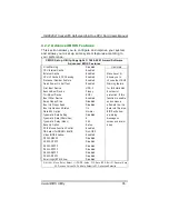
DRAM Timing By SPD
This item allows you to select the value in this field,
depending on whether the board has paged DRAMs or
EDO (extended data output) DRAMs.
DRAM Clock
This item allows you to select the DRAM clock value,
depending on whether the board has paged DRAMs or
EDO (extended data output) DRAMs. The available choices
are 66 MHz and Host CLK.
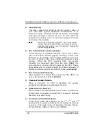
SDRAM Cycle Length
When synchronous DRAM is installed, the number of clock
cycles of CAS latency depends on the DRAM timing. Do
not reset this field from the default value specified by the
system designer. The default setting is
3
.
Memory Hole
To improve performance, certain space in memory is
reserved for ISA cards. This memory must be mapped into
the memory space below 16MB. The available choices are
15M-16M and Disabled.
P2C/C2P Concurrency
This item allows you to enable/disable the PCI to CPU,
CPU to PCI concurrency. By default, this field is set to
Enabled
.
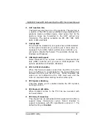
System BIOS Cacheable
When enabled, access to the system BIOS ROM addressed
at F0000H-FFFFFH is cached, provided that the cache
controller is disabled.
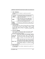
Video RAM Cacheable
Selecting
Enabled
allows caching of the video BIOS ROM
at C0000h to C7FFFh, resulting in better video
performance. However, if any program writes to this
memory area, a memory access error may result.
Award BIOS Utility
40


