


3-Feb-2015
6
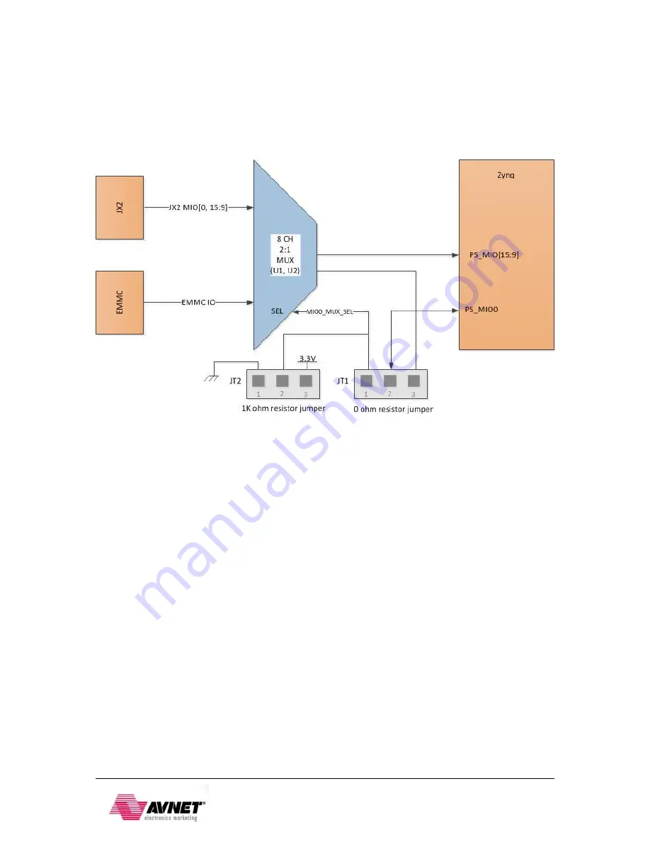
If JT2 resistor jumper position is changed to position 2-3, the JX2 MIO pins become selected by
the multiplexers. In this case, it is best to also change the JT1 jumper position to 2-3 to ensure
that a full 8-bit peripheral can be connected through the JX2 MIO interface if so desired.
The diagram below shows how the eMMC and JX2 MIO signals are connected to the Zynq via
the multiplexer ICs U1 and U2.
Figure 2
– eMMC / JX2 MIO Multiplexer Block Diagram
2.3 USB 2.0 OTG
Zynq contains a hardened PS USB 2.0 controller. PicoZed 7010/7020 takes advantage of the
USB 2.0 controller to provide USB 2.0 On-The-Go signaling to the JX3 connector.
PicoZed 7010/7020 implements one of the two available PS USB 2.0 interfaces. An external
PHY with an 8-bit ULPI interface is implemented. A SMSC USB3320 Standalone USB
Transceiver Chip is used as the PHY. The PHY features a complete HS-USB Physical Front-End
supporting speeds of up to 480Mbs. VDDIO for this device can be 1.8V or 3.3V, and on the
PicoZed 7010/7020 is powered at 1.8V. The PHY is connected to MIO Bank 1/501, which is also
powered at 1.8V. This is critical since a level translator cannot be used as it would impact the
tight ULPI timing required between the PHY and the Zynq device.
Additionally the USB chip must clock the ULPI interface which requires a 24 MHz crystal or
oscillator (configured as ULPI Output Clock Mode). On the PicoZed 7010/7020, the 24 MHz
oscillator is an Abracon ASDMB CMOS oscillator, ASDMB-24.000MHZ-LC-T.
The USB connector is not populated on the PicoZed 7010/7020 System-on-Module and is
designed to have the USB connector reside on the mating carrier card. The four USB connector
signals (USB_P, USB_N, USB_ID and USB_OTG_CPEN) are connected to the JX3 Micro
Header. The table below shows the connections of these four signals at JX3.


