background image

329

8331B–AVR–03/12

Atmel AVR XMEGA AU

26.3

Operation

The data source for the CRC module must be selected in software as either flash memory, the
DMA channels, or the I/O interface. The CRC module then takes data input from the selected
source and generates a checksum based on these data. The checksum is available in the
CHECKSUM registers in the CRC module. When CRC-32 polynomial is used, the final check-
sum read is bit reversed and complemented (see 

Figure 26-1

).

For the I/O interface or DMA controller, which CRC polynomial is used is software selectable,
but the default setting is CRC-16. CRC-32 is automatically used if Flash Memory is selected as
the source. The CRC module operates on bytes only.

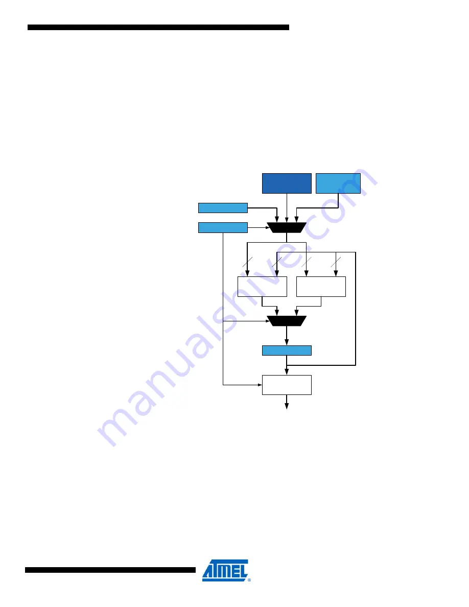
Figure 26-1.

CRC generator block diagram.

26.4

CRC on Flash memory

A CRC-32 calculation can be performed on the entire flash memory, on only the application sec-
tion, on only the boot section, or on a software selectable range of the flash memory. Other than
selecting the flash as the source, all further control and setup are done from the NVM controller.
This means that the NVM controller configures the memory range to perform the CRC on, and
the CRC is started using NVM commands. Once completed, the result is available in the check-
sum registers in the CRC module. For further details on setting up and performing CRC on flash
memory, refer to 

”Memory Programming” on page 431

.

DATAIN

CTRL

Flash

Memory

DMA

Controller

CRC-16

CRC-32

CHECKSUM

bit-r

complement

16

8

8

32

Checksum read

crc32

Содержание AVR XMEGA AU series

Страница 1: ...l interrupt controller PORT I O ports TC 16 bit timer counters AWeX Advanced waveform extension Hi Res High resolution extension RTC Real time counter RTC32 32 bit real time counter USB Universial ser...

Страница 2: ...tion sections list all registers and describe each register bit and flag with their function This includes details on how to set up and enable various features in the module When multiple bits are nee...

Страница 3: ...L and prescaler and programmable brown out detection The program and debug interface PDI a fast two pin interface for programming and debug ging is available Selected devices also have an IEEE std 114...

Страница 4: ...A DACB ADCB ACB OCD PORT K 8 PORT J 8 PORT H 8 PDI Watchdog Timer Watchdog Oscillator Interrupt Controller DATA BUS Prog Debug Controller PORT R 2 Oscillator Circuits Clock Generation Oscillator Contr...

Страница 5: ...28 Boot memory KB 4 8 4 8 8 4 8 SRAM KB 4 8 4 16 16 2 8 EEPROM 2 2 4 4 1 2 General purpose registers 16 16 16 16 Package TQFP 100A 64A 64A 44A QFN VQFN 64M2 64M2 44M1 BGA 100C1 100C2 49C2 QTouch Sense...

Страница 6: ...es Analog to Digital Converter ADC 2 2 2 1 Resolution bits 12 12 12 12 Sampling speed kbps 2000 2000 2000 2000 Input channels per ADC 16 16 16 12 Conversion channels 4 4 4 4 Digital to Analog Converte...

Страница 7: ...to access memories perform calculations control peripherals and execute the program in the flash memory Interrupt han dling is described in a separate section Interrupts and Programmable Multilevel In...

Страница 8: ...from SRAM is not supported It can easily be accessed through the five different addressing modes supported in the AVR architecture The first SRAM address is 0x2000 Data addresses 0x1000 to 0x1FFF are...

Страница 9: ...2 bit format During interrupts and subroutine calls the return address PC is stored on the stack The stack is allocated in the general data SRAM and consequently the stack size is only limited by the...

Страница 10: ...always points to the top of the stack It is implemented as two 8 bit registers that are accessible in the I O memory space Data are pushed and popped from the stack using the PUSH and POP instruction...

Страница 11: ...s register pointers for data space addressing enabling efficient address calculations One of these address pointers can also be used as an address pointer for lookup tables in flash program memory Fig...

Страница 12: ...y the number of bits required to address the whole program and data memory space in the device is implemented in the registers 3 10 1 RAMPX RAMPY and RAMPZ Registers The RAMPX RAMPY and RAMPZ register...

Страница 13: ...low byte register is read by the CPU the high byte of the 16 bit register is copied into the temporary register in the same clock cycle as the low byte is read When the high byte is read it is then r...

Страница 14: ...execution of protected SPM LPM 1 The application code writes the signature for the execution of protected SPM LPM to the CCP register 2 Within four instruction cycles the application code must execut...

Страница 15: ...gister is concatenated with the operand for direct addressing LDS STS of the whole data memory space on devices with more than 64KB of data memory This register is not avail able if the data memory in...

Страница 16: ...than 64KB of data memory RAMPZ is concat enated with the Z register when reading ELPM program memory locations above the first 64KB and writing SPM program memory locations above the first 128KB of th...

Страница 17: ...m software a write to SPL will automatically disable interrupts for the next four instructions or until the next I O mem ory write Only the number of bits required to address the available data memory...

Страница 18: ...bit in a register in the register file by the BLD instruction Bit 5 H Half Carry Flag The half carry flag H indicates a half carry in some arithmetic operations Half carry Is useful in BCD arithmetic...

Страница 19: ...Bit 0 Page 0x00 Reserved 0x01 Reserved 0x02 Reserved 0x03 Reserved 0x04 CCP CCP 7 0 15 0x05 Reserved 0x06 Reserved 0x07 Reserved 0x08 RAMPD RAMPD 7 0 15 0x09 RAMPX RAMPX 7 0 15 0x0A RAMPY RAMPY 7 0 16...

Страница 20: ...andling of priority between CPU DMA controller and other bus masters Separate buses for SRAM EEPROM I O memory and external memory access Simultaneous bus access for CPU and DMA controller Production...

Страница 21: ...SPM instruction used to write to the flash from the application software will only operate when executed from the boot loader section The application section contains an application table section with...

Страница 22: ...ch manufactured device The serial number consists of the production lot number wafer number and wafer coordinates for the device The production signature row cannot be written or erased but it can be...

Страница 23: ...SRAM always starts at hexadecimal address 0x2000 SRAM is accessed by the CPU using the load LD LDS LDD and store ST STS STD instructions 4 7 EEPROM All XMEGA devices have EEPROM for nonvolatile data...

Страница 24: ...External Memory Up to four ports are dedicated to external memory supporting external SRAM SDRAM and memory mapped peripherals such as LCD displays For details refer to EBI External Bus Interface on p...

Страница 25: ...er to the instruction summary for more details on instructions and instruction timing 4 12 Device ID and Revision Each device has a three byte device ID This ID identifies Atmel as the manufacturer of...

Страница 26: ...This register gives the address extended byte when accessing NVM locations 4 15 4 DATA0 Data register 0 The DATA0 DATA1 and DATA registers represent the 24 bit value DATA This holds data dur ing NVM r...

Страница 27: ...ands for the flash Bit 6 is only set for external pro gramming commands See Memory Programming on page 431 for programming commands 4 15 8 CTRLA Control register A Bit 7 1 Reserved These bits are unus...

Страница 28: ...d the CPU will be halted for a time equal to the start up time from the idle sleep mode Bit 1 EPRM EEPROM Power Reduction Mode Setting this bit enables power saving for the EEPROM The EEPROM will then...

Страница 29: ...sh EEPROM lockbit is being programmed Once an operation is started this flag is set and remains set until the operation is completed The NVMBUSY flag is automatically cleared when the operation is fin...

Страница 30: ...of the NVM lock bits into the I O memory space which enable direct read access from the application software Refer to LOCKBITS Lock Bit register on page 35 for description Bit 7 6 5 4 3 2 1 0 0x07 BL...

Страница 31: ...etails Bit 3 0 WDPER 3 0 Watchdog Timeout Period These fuse bits are used to set the initial value of the watchdog timeout period During reset these fuse bits are automatically written to the PER bits...

Страница 32: ...ation in Power down Mode These fuse bits set the BOD operation mode in all sleep modes except idle mode For details on the BOD and BOD operation modes refer to Brownout Detection on page 115 4 16 4 FU...

Страница 33: ...the watchdog timer configuration cannot be changed and the ENABLE bit in the watchdog CTRL register is automatically set at reset and cannot be cleared from the appli cation software The WEN bit in t...

Страница 34: ...independent of the software revision Changes to the EESAVE fuse bit take effect immediately after the write timeout elapses Hence it is possible to update EESAVE and perform a chip erase according to...

Страница 35: ...Write R W R W R W R W R W R W R W R W Initial Value 1 1 1 1 1 1 1 1 Table 4 9 Boot lock bit for the boot loader section BLBB 1 0 Group Configuration Description 11 NOLOCK No lock no restrictions for...

Страница 36: ...ed while executing from the application section 00 RWLOCK Read and write lock SPM is not allowed to write to the application section and E LPM executing from the boot loader section is not allowed to...

Страница 37: ...7 0 RCOSC2MA 7 0 Internal 2MHz Oscillator Calibration Value This byte contains the oscillator calibration value for the internal 2MHz oscillator Calibration of the oscillator is performed during produ...

Страница 38: ...ster B for the 32MHz DFLL Refer to CALB DFLL Calibration register B on page 102 for more details 4 17 5 RCOSC32MA Internal 32MHz RC Oscillator Calibration register Bit 7 0 RCOSC32MA 7 0 Internal 32MHz...

Страница 39: ...the lot number for the device 4 17 9 LOTNUM3 Lot Number register 3 Bit 7 0 LOTNUM3 7 0 Lot Number Byte 3 This byte contains byte 3 of the lot number for the device Bit 7 6 5 4 3 2 1 0 0x08 LOTNUM0 7...

Страница 40: ...OORDX0 Wafer Coordinate X register 0 COORDX0 COORDX1 COORDY0 and COORDY1 contain the wafer X and Y coordinates for each device Together with the lot number and wafer number this gives a serial number...

Страница 41: ...Calibration is done dur ing production to enable operation without requiring external components on the USB lines for the device The calibration bytes are not loaded automatically into the USB calibra...

Страница 42: ...on register 0 ADCACAL0 and ADCACAL1 contain the calibration value for the analog to digital converter A ADCA Calibration is done during production test of the device The calibration bytes are not load...

Страница 43: ...t 7 0 ADCBCAL0 7 0 ADCB Calibration Byte 1 This byte contains byte 1 of the ADCB calibration data and must be loaded into the ADCB CALH register 4 17 24 TEMPSENSE0 Temperature Sensor Calibration regis...

Страница 44: ...for channel 0 in the digital to analog converter A DACA Calibration is done during production test of the device The calibration byte is not loaded automatically into the DAC gain calibration register...

Страница 45: ...nverter A DACA Calibration is done during production test of the device The calibration byte is not loaded automatically into the DAC channel 1 offset calibration register so this must be done from so...

Страница 46: ...libration is done during production test of the device The calibration byte is not loaded automatically into the DAC channel 1 gain calibration register so this must be done from software 4 18 Registe...

Страница 47: ...of the device ID indicates the flash size of the device 4 20 3 DEVID2 Device ID register 2 Bit 7 0 DEVID2 7 0 Device ID Byte 2 Byte 2 of the device ID indicates the device number 4 20 4 REVID Revision...

Страница 48: ...etails refer to Configuration Change Protection on page 13 4 20 7 ANAINIT Analog Initialization register Bit 7 4 Reserved These bits are unused and reserved for future use For compatibility with futur...

Страница 49: ...e 13 Bit 3 1 Reserved These bits are unused and reserved for future use For compatibility with future devices always write these bits to zero when this register is written Bit 0 EVSYS0LOCK Setting thi...

Страница 50: ...protected by the configuration change protection mechanism For details refer to Configuration Change Protection on page 13 Bit 1 Reserved This bit is unused and reserved for future use For compatibili...

Страница 51: ...Reserved 0x0A CMD CMD 6 0 26 0x0B CTRLA CMDEX 27 0x0C CTRLB EEMAPEN FPRM EPRM SPMLOCK 27 0x0D INTCTRL SPMLVL 1 0 EELVL 1 0 28 0x0E Reserved 0x0F STATUS NVMBUSY FBUSY EELOAD FLOAD 28 0x10 LOCKBITS BLBB...

Страница 52: ...41 0x16 Reserved 0x17 Reserved 0x18 Reserved 0x19 Reserved 0x1A USBCAL0 USBCAL0 7 0 41 0x1B USBCAL1 USBCAL1 7 0 42 0x1C RCOSC48M RCOSC48M 7 0 42 0x1D Reserved 0x0E Reserved 0x1E Reserved 0x20 NO ADCAC...

Страница 53: ...6 0x0C GPIOR12 GPIOR 7 0 46 0x0D GPIOR13 GPIOR 7 0 46 0x0E GPIOR14 GPIOR 7 0 46 0x0F GPIOR15 GPIOR 7 0 46 Address Name Bit 7 Bit 6 Bit 5 Bit 4 Bit 3 Bit 2 Bit 1 Bit 0 Page 0x00 DEVID0 DEVID0 7 0 47 0x...

Страница 54: ...ers The DMA controller can move data between SRAM and peripherals between SRAM locations and directly between peripheral registers With access to all peripherals the DMA controller can handle automati...

Страница 55: ...urst Transfer Since the AVR CPU and DMA controller use the same data buses a block transfer is divided into smaller burst transfers The burst transfer is selectable to 1 2 4 or 8 bytes This means that...

Страница 56: ...require a transfer trigger It will start as soon as the previous block is done If the trigger source generates a transfer request during an ongoing transfer this will be kept pending and the transfer...

Страница 57: ...ecessary bus loading when doing data transfer between memories with different access timing for example I O register and external memory the DMA controller has a four byte buffer Two bytes will be rea...

Страница 58: ...on is complete for a DMA channel Each DMA channel has a separate interrupt vector and there are different interrupt flags for error and transaction complete If repeat is not enabled the transaction co...

Страница 59: ...FMODE 1 0 Double Buffer Mode These bits enable the double buffer on the different channels according to Table 5 1 Bit 1 0 PRIMODE 1 0 Channel Priority Mode These bits determine the internal channel pr...

Страница 60: ...lock transfer is pending on DMA channel n the CHnPEND flag will be read as one This flag is automatically cleared when the block transfer starts or if the transfer is aborted 5 13 4 TEMPL Temporary re...

Страница 61: ...t Setting this bit will reset the DMA channel It can only be set when the DMA channel is disabled CHEN 0 Writing a one to this bit will be gnored as long as the channel is enabled CHEN 1 This bit is a...

Страница 62: ...ation Description 00 1BYTE 1 byte burst mode 01 2BYTE 2 bytes burst mode 10 4BYTE 4 bytes burst mode 11 8BYTE 8 bytes burst mode Table 5 4 Summary of triggers transcation complete flag and channel dis...

Страница 63: ...saction is complete and TRNIFR is set after the block transfer When unlimited repeat is enabled TRNIF is also set after each block transfer Since the DMA channel transaction n complete interrupt share...

Страница 64: ...l source address reload settings SRCRELOAD 1 0 Group Configuration Description 00 NONE No reload performed 01 BLOCK DMA source address register is reloaded with initial value at end of each block tran...

Страница 65: ...evel enabled so that an interrupt is triggered the DMA request will be lost Since a DMA request can clear the interrupt flag interrupts can be lost Note For most trigger sources the request is cleared...

Страница 66: ...A triggers base value 0x8E USARTE1 USART E1 DMA triggers base value 0xA0 TCF0 Timer counter F0 DMA triggers base value 0xA6 TCF1 Timer counter F1 triggers base value 0xAA SPIF SPI F DMA trigger value...

Страница 67: ...register and fires a DMA trig ger DMA will be doing 0xFFFF transfers 5 14 6 TRFCNTH Channel Block Transfer Count register H Reading and writing 16 bit values requires special attention For details ref...

Страница 68: ...e last block transfer is completed Unlimited repeat is achieved by setting this register to zero 5 14 8 SRCADDR0 Source Address 0 SRCADDR0 SRCADDR1 and SRCADDR2 represent the 24 bit value SRCADDR whic...

Страница 69: ...f the 24 bit source address 5 14 12 DESTADDR1 Channel Destination Address 1 Bit 7 0 DESTADDR 15 8 Channel Destination Address 1 These bits hold byte 1 of the 24 bit source address 5 14 13 DESTADDR2 Ch...

Страница 70: ...6 Bit 5 Bit 4 Bit 3 Bit 2 Bit 1 Bit 0 Page 0x00 CTRLA ENABLE RESET REPEAT TRFREQ SINGLE BURSTLEN 1 0 61 0x01 CTRLB CHBUSY CHPEND ERRIF TRNIF ERRINTLVL 1 0 TRNINTLVL 1 0 63 0x02 ADDCTRL SRCRELOAD 1 0 S...

Страница 71: ...predictable response times between peripherals It allows for autonomous peripheral control and interaction without the use of inter rupts CPU or DMA controller resources and is thus a powerful tool f...

Страница 72: ...tate within a peripheral has occurred is called an event There are two main types of events signaling events and data events Signaling events only indicate a change of state while data events contain...

Страница 73: ...can also use signaling events This is configurable and is described in the datasheet module for each peripheral 6 3 3 Peripheral Clock Events Each event channel includes a peripheral clock prescaler w...

Страница 74: ...tiplex ers CHnMUX which can each be configured to route any event source to any event users The output from a multiplexer is referred to as an event channel For each peripheral it is selectable if and...

Страница 75: ...rk configuration itself is compatible between all devices 48 PORTA PORTB PORTC PORTD PORTE PORTF ADCA ADCB DACA DACB TCF0 TCF1 6 4 TCE0 TCE1 6 4 TCD0 TCD1 6 4 TCC0 TCC1 6 4 8 8 8 10 10 10 10 36 4 4 8...

Страница 76: ...tended for pin change events 6 7 Quadrature Decoder The event system includes three quadrature decoders QDECs which enable the device to decode quadrature input on I O pins and send data events that a...

Страница 77: ...l index count The following procedure should be used for QDEC setup 1 Choose two successive pins on a port as QDEC phase inputs 2 Set the pin direction for QDPH0 and QDPH90 as input 3 Set the pin conf...

Страница 78: ...eripheral is present or not Selecting event sources from peripherals that are not present will give the same result as when this register is zero When this register is zero no events are routed throug...

Страница 79: ...111 1 n PORTF_PINn 1 PORTF pin n n 0 1 2 or 7 1000 M PRESCALER_M ClkPER divide by 2M M 0 to 15 1001 X X X X Reserved 1010 X X X X Reserved 1011 X X X X Reserved 1100 0 E See Table 6 4 Timer counter C0...

Страница 80: ...ed This bit is available only for CH0CTRL CH2CTRL and CH4CTRL Bit 3 QDEN Quadrature Decode Enable Setting this bit enables QDEC operation This bit is available only for CH0CTRL CH2CTRL and CH4CTRL Bit...

Страница 81: ...r must be written before the STROBE register For details See STROBE Strobe register on page 81 Table 6 6 Digital filter coefficient values DIGFILT 2 0 Group Configuration Description 000 1SAMPLE One s...

Страница 82: ...CH4MUX CH4MUX 7 0 78 0x05 CH5MUX CH5MUX 7 0 78 0x06 CH6MUX CH6MUX 7 0 78 0x07 CH7MUX CH7MUX 7 0 78 0x08 CH0CTRL QDIRM 1 0 QDIEN QDEN DIGFILT 2 0 80 0x09 CH1CTRL DIGFILT 2 0 80 0x0A CH2CTRL QDIRM 1 0 Q...

Страница 83: ...al oscillators and external crystal oscillator and resonator sup port A high frequency phase locked loop PLL and clock prescalers can be used to generate a wide range of clock frequencies A calibratio...

Страница 84: ...Volatile Memory Watchdog Timer Brown out Detector System Clock Prescalers USB Prescaler System Clock Multiplexer SCLKSEL PLLSRC RTCSRC DIV32 32 kHz Int ULP 32 768 kHz Int OSC 32 768 kHz TOSC 2 MHz In...

Страница 85: ...oscillator The dedicated clock domain allows operation of this peripheral even when the device is in sleep mode and the rest of the clocks are stopped 7 3 6 USB Clock ClkUSB The USB device module req...

Страница 86: ...clock source 7 4 1 4 2MHz Run time Calibrated Oscillator The 2MHz run time calibrated internal oscillator is the default system clock source after reset It is calibrated during production to provide...

Страница 87: ...ctable from software and can be changed during normal operation Built in hardware protection prevents unsafe clock switching It is not possible to select a non stable or disabled oscillator as the clo...

Страница 88: ...1 to 31 The output frequency fOUT is given by the input frequency fIN multiplied by the multiplication factor PLL_FAC Four different clock sources can be chosen as input to the PLL 2MHz internal osci...

Страница 89: ...for each DFLL as shown on Figure 7 6 on page 89 Figure 7 6 DFLL reference clock selection The ideal counter value representing the frequency ratio between the internal oscillator and a 1 024kHz refere...

Страница 90: ...ue of the DFLL calibration register can be read from the production signature row When the DFLL is disabled the DFLL calibration register can be written from software for man ual run time calibration...

Страница 91: ...t cannot be used for slower external clocks When the failure monitor is enabled it will not be disabled until the next reset The failure monitor is stopped in all sleep modes where the PLL or external...

Страница 92: ...ot stable The old clock can not be dis abled until the clock switching is completed 7 9 2 PSCTRL Prescaler register This register is protected by the configuration change protection mechanism For deta...

Страница 93: ...k frequency for the ClkPER and ClkCPU clocks relative to the ClkPER2 clock Refer to Figure 7 5 on page 88 fore more details Table 7 2 Prescaler A division factor PSADIV 4 0 Group Configuration Descrip...

Страница 94: ...bits are unused and reserved for future use For compatibility with future devices always write these bits to zero when this register is written Bit 3 1 RTCSRC 2 0 RTC Clock Source These bits select t...

Страница 95: ...t the clock source for the USB module according to Table 7 6 on page 95 Note 1 The 32MHz internal oscillator must be calibrated to 48MHz before selecting this as source for the USB device module Refer...

Страница 96: ...for the system clock See STATUS Oscillator Status register on page 97 Bit 2 RC32KEN 32 768kHz Internal Oscillator Enable Setting this bit enables the 32 768kHz internal oscillator The oscillator must...

Страница 97: ...ready to be used as the system clock source Bit 1 RC32MRDY 32MHz Internal Oscillator Ready This flag is set when the 32MHz internal oscillator is stable and is ready to be used as the sys tem clock s...

Страница 98: ...ck see CTRL Oscillator Control register on page 96 This configuration cannot be changed Notes 1 This option should be used only when frequency stability at startup is not important for the application...

Страница 99: ...ll clear XOSCFDIF Bit 0 XOSCFDEN Failure Detection Enable Setting this bit will enable the failure detection monitor and a non maskable interrupt will be issued when XOSCFDIF is set This bit is protec...

Страница 100: ...For compatibility with future devices always write these bits to zero when this register is written Bit 2 1 RC32MCREF 1 0 32MHz Oscillator Calibration Reference These bits are used to select the cali...

Страница 101: ...rnal oscillator The reference clock must be enabled and stable before the DFLL is enabled After disabling the DFLL the reference clock can not be disabled before the ENABLE bit is read as zero 7 11 2...

Страница 102: ...is used to select the oscillator fre quency A factory calibrated value is loaded from the signature row of the device and written to this register during reset giving an oscillator frequency approxima...

Страница 103: ...4 3 2 1 0 0x06 COMP 15 8 COMP2 Read Write R W R W R W R W R W R W R W R W Initial Value 0 0 0 0 0 0 0 0 Table 7 11 Nominal DFLL32M COMP values for different output frequencies Oscillator Frequency MHz...

Страница 104: ...N RC2MEN 96 0x01 STATUS PLLRDY XOSCRDY RC32KRDY R32MRDY RC2MRDY 96 0x02 XOSCCTRL FRQRANGE 1 0 X32KLPM XOSCPWR XOSCSEL 3 0 97 0x03 XOSCFAIL PLLFDIF PLLFDEN XOSCFDIF XOSCFDEN 99 0x04 RC32KCAL RC32KCAL 7...

Страница 105: ...ripherals from software When this is done the current state of the peripheral is frozen and there is no power consumption from that peripheral This reduces the power consumption in active mode and idl...

Страница 106: ...kept running Any enabled interrupt will wake the device 8 3 2 Power down Mode In power down mode all clocks including the real time counter clock source are stopped This allows operation only of async...

Страница 107: ...ption in an AVR MCU controlled system In general correct sleep modes should be selected and used to ensure that only the modules required for the application are operating All unneeded functions shoul...

Страница 108: ...power Refer to WDT Watchdog Timer on page 128 for details on how to configure the watchdog timer 8 5 5 Port Pins When entering a sleep mode all port pins should be configured to use minimum power Mos...

Страница 109: ...d unintentional entering of sleep modes it is recommended to write SEN just before executing the SLEEP instruction and clear it immediately after waking up 8 7 Register Description Power Reduction 8 7...

Страница 110: ...to ensure proper operation Bit 2 RTC Real Time Counter Setting this bit stops the clock to the real time counter When this bit is cleared the peripheral should be reinitialized to ensure proper opera...

Страница 111: ...r operation Bit 4 USART0 Setting this bit stops the clock to USART0 When this bit is cleared the peripheral should be reinitialized to ensure proper operation Bit 3 SPI Serial Peripheral Interface Set...

Страница 112: ...L SMODE 2 0 SEN 109 Address Name Bit 7 Bit 6 Bit 5 Bit 4 Bit 3 Bit 2 Bit 1 Bit 0 Page 0x00 PRGEN USB AES EBI RTC EVSYS DMA 109 0x01 PRPA DAC ADC AC 110 0x02 PRPB DAC ADC AC 110 0x03 PRPC TWI USART1 US...

Страница 113: ...re immediately tri stated The program counter is set to the reset vector location and all I O registers are set to their initial values The SRAM content is kept However if the device accesses the SRAM...

Страница 114: ...when all reset requests are released The reset delay is timed from the 1kHz output of the ultra low power ULP internal oscillator and in addition 24 System clock clkSYS cycles are counted before rese...

Страница 115: ...VPOT and this will start the reset sequence The POR is also activated to power down the device properly when the VCC falls and drops below the VPOT level The VPOT level is higher for falling VCCthan...

Страница 116: ...the trigger level for lon ger than tBOD Figure 9 4 Brownout detection reset For BOD characterization data consult the device datasheet The programmable BODLEVEL setting is shown in Table 9 2 Notes 1 T...

Страница 117: ...e mode while the BODPD fuse determines the brownout detection setting for all sleep modes except idle mode 9 4 3 External Reset The external reset circuit is connected to the external RESET pin The ex...

Страница 118: ...ster The reset will be issued within two CPU clock cycles after writing the bit It is not possible to execute any instruction from when a software reset is requested until it is issued Figure 9 7 Soft...

Страница 119: ...ccurs The flag will be cleared by a power on reset or by writ ing a one to the bit location Bit 1 EXTRF External Reset Flag This flag is set if an external reset occurs The flag will be cleared by a p...

Страница 120: ...120 8331B AVR 03 12 Atmel AVR XMEGA AU 9 6 Register Summary Address Name Bit 7 Bit 6 Bit 5 Bit 4 Bit 3 Bit 2 Bit 1 Bit 0 Page 0x00 STATUS SRF PDIRF WDRF BORF EXTRF PORF 119 0x01 CTRL SWRST 119...

Страница 121: ...switching between main power and a battery backup power supply No external components are required Figure 10 1 on page 122 shows an overview of the system On devices with a battery backup system a bac...

Страница 122: ...e VBAT voltage drops below a threshold voltage the battery backup bod flag BBBODF is set The BBBOD samples the VBAT voltage level at around a 1Hz rate and is designed for detecting slow voltage change...

Страница 123: ...ess enable bit 3 Optionally configure the oscillator output and ESR selection 4 Optionally enable the crystal oscillator failure monitor and the required delay before continuing configuration 5 Enable...

Страница 124: ...power supervision flags are cleared the battery backup system runs as nor mal The software should enable access to the battery backup system and check the crystal oscillator failure flag If the flag...

Страница 125: ...described in Configuration on page 123 Bit 2 XOSCFDEN Crystal Oscillator Failure Detection Enable Setting this bit will enable the crystal oscillator monitor The monitor will detect if the crystal is...

Страница 126: ...cillator failure is detected The flag can be cleared by writing a one to this bit location or by applying a reset to the battery backup system Bit 1 BBBODF Battery Backup Brown out Detection Flag This...

Страница 127: ...register can be used to store data in the battery backup system before the main power is lost or removed 10 7 Register Summary Bit 7 6 5 4 3 2 1 0 0x03 BACKUP1 7 0 BACKUP1 Read Write R W R W R W R W R...

Страница 128: ...ch WDT must be reset If the WDT is reset outside this window either too early or too late a system reset will be issued Compared to the normal mode this can also catch sit uations where a code error c...

Страница 129: ...o the total duration of the time out period is the sum of the closed window and the open window timeout periods The default closed window timeout period is controlled by fuses both open and closed per...

Страница 130: ...ster Bits 7 6 Reserved These bits are unused and reserved for future use For compatibility with future devices always write these bits to zero when this register is written Bits 5 2 PER 3 0 Timeout Pe...

Страница 131: ...mecha nism For a detailed description refer to Configuration Change Protection on page 13 11 7 2 WINCTRL Window Mode Control register Bit 7 6 Reserved These bits are unused and reserved for future use...

Страница 132: ...me This bit is protected by the configuration change protection mechanism For a detailed description refer to Configuration Change Protection on page 13 Bit 0 WCEN Window Mode Change Enable This bit e...

Страница 133: ...registers and the data are being synchro nized from the system clock to the WDT clock domain This bit is automatically cleared after the synchronization is finished Synchronization will take place onl...

Страница 134: ...the interrupt priority is decided from the interrupt vector address where the lowest interrupt vector address has the highest interrupt priority Low level interrupts have an optional round robin sche...

Страница 135: ...or written This is described for each individual interrupt flag If an interrupt condition occurs while another higher priority interrupt is executing or pending the interrupt flag will be set and rem...

Страница 136: ...same time priority is static according to the interrupt vector address where the lowest address has highest priority 12 4 2 Interrupt Response Time The interrupt response time for all the enabled int...

Страница 137: ...tion response time is increased by five clock cycles In addition the response time is increased by the start up time from the selected sleep mode A return from an interrupt handling routine takes four...

Страница 138: ...is decided both by the level and the pri ority of the interrupt request Interrupts can be organized in a static or dynamic round robin priority scheme High and medium level interrupts and the NMI wil...

Страница 139: ...enabled the interrupt vector address for the last acknowledged low level interrupt will have the lowest priority the next time one or more interrupts from the low level is requested Figure 12 4 Round...

Страница 140: ...Vectors are not used and regular program code can be placed at these locations This is also the case if the Reset Vector is in the Application section while the Interrupt Vectors are in the Boot sect...

Страница 141: ...turning RETI from the interrupt handler Bit 0 LOLVLEX Low level Interrupt Executing This flag is set when a low level interrupt is executing or when the interrupt handler has been interrupted by an in...

Страница 142: ...ure use For compatibility with future devices always write these bits to zero when this register is written Bit 2 HILVLEN High level Interrupt Enable 1 When this bit is set all high level interrupts a...

Страница 143: ...ontrollers have flexible general purpose I O ports One port consists of up to eight port pins pin 0 to 7 Each port pin can be configured as input or output with configurable driver and pull settings T...

Страница 144: ...ritten to one pin n is configured as an output pin If DIRn is written to zero pin n is configured as an input pin When direction is set as output the OUTn bit in OUT is used to set the value of the pi...

Страница 145: ...onfiguration is configured through the pin configuration register all intermediate port states during switching of the pin direction and pin values are avoided The I O pin configurations are summarize...

Страница 146: ...s 1 the bus keeper configuration will use the internal pull resistor to keep the bus high If the last logic level on the pin bus was 0 the bus keeper will use the internal pull resistor to keep the bu...

Страница 147: ...set as input Figure 13 7 Output configuration Wired AND with optional pull up 13 4 Reading the Pin Value Independent of the pin data direction the pin value can be read from the IN register as shown i...

Страница 148: ...erted input configuration Input sensing can be used to trigger interrupt requests IREQ or events when there is a change on the pin The I O pins support synchronous and asynchronous input sensing Synch...

Страница 149: ...e will still wake up but no interrupt request will be generated A low level can always be detected by all pins regardless of a peripheral clock being present or not If a pin is configured for low leve...

Страница 150: ...I O pin When an alternate function is enabled it might override the normal port pin function or pin value This happens when other peripherals that require pins are enabled or configured to use pins I...

Страница 151: ...e peripheral clock and event channel 0 events to a pin This can be used to clock control and synchronize external functions and hardware to internal device tim ing The output port pin is selectable If...

Страница 152: ...being written the same way during identical write operations 13 12 Virtual Ports Virtual port registers allow the port registers to be mapped virtually in the bit accessible I O memory space When thi...

Страница 153: ...he DIR register 13 13 3 DIRCLR Data Direction Clear register Bit 7 0 DIRCLR 7 0 Port Data Direction Clear This register can be used instead of a read modify write to set individual pins as input Writi...

Страница 154: ...This register can be used instead of a read modify write to set the output value of individual pins to one Writing a one to a bit will set the corresponding bit in the OUT register Reading this reg i...

Страница 155: ...Interrupt Control Register Bit 7 4 Reserved These bits are unused and reserved for future use For compatibility with future devices always write these bits to zero when this register is written Bit 3...

Страница 156: ...The INTnIF flag is set when a pin change state matches the pin s input sense configuration and the pin is set as source for port interrupt n Writing a one to this flag s bit location will clear the fl...

Страница 157: ...tputs Bit 0 TC0A Timer Counter 0 Output Compare A Setting this bit will move the location of OC0A from Px0 to Px4 If this bit is set and PWM from both timer counter 0 and timer counter 1 is enabled th...

Страница 158: ...y such as AC or ADC it is recommended to configure the pin to INPUT_DISABLE Table 13 5 Output pull configuration OPC 2 0 Group Configuration Description Output Configuration Pull Configuration 000 TOT...

Страница 159: ...ters is equal to accessing the actual port registers See Table 13 7 for configuration Bit 3 0 VP0MAP Virtual Port 0 Mapping These bits decide which ports should be mapped to Virtual Port 0 The registe...

Страница 160: ...ently from those of EVOUT The port pin must be configured as output for the event to be available on the pin Table 13 7 Virtual port mapping VPnMAP 3 0 Group Configuration Description 0000 PORTA PORTA...

Страница 161: ...ut register Bit 7 4 Reserved These bits are unused and reserved for future use For compatibility with future devices always write these bits to zero when this register is written Table 13 8 Event outp...

Страница 162: ...future use For compatibility with future devices always write these bits to zero when this register is written Bit 2 0 EVOUTSEL 2 0 Event Channel Output Selection These bits define which channel from...

Страница 163: ...uration Description 000 0 Event channel 0 output to pin 001 1 Event channel 1 output to pin 010 2 Event channel 2 output to pin 011 3 Event channel 3 output to pin 100 4 Event channel 4 output to pin...

Страница 164: ...register B When a port is mapped as virtual accessing this register is identical to accessing the actual OUT register for the port 13 15 3 IN Data Input Value Bit 7 0 IN 7 0 Data Input Value This regi...

Страница 165: ...nd the pin is set as source for port interrupt n Writing a one to this flag s bit location will clear the flag For enabling and executing the interrupt refer to the interrupt level description The con...

Страница 166: ...SRLEN INVEN OPC 2 0 ISC 2 0 157 0x12 PIN2CTRL SRLEN INVEN OPC 2 0 ISC 2 0 157 0x13 PIN3CTRL SRLEN INVEN OPC 2 0 ISC 2 0 157 0x14 PIN4CTRL SRLEN INVEN OPC 2 0 ISC 2 0 157 0x15 PIN5CTRL SRLEN INVEN OPC...

Страница 167: ...A AU 13 19 Interrupt Vector Summary Ports Table 13 15 Port interrupt vectors and their word offset address Offset Source Interrupt Description 0x00 INT0_vect Port interrupt vector 0 offset 0x02 INT1_v...

Страница 168: ...ut with programmable dead time insertion DTI Event controlled fault protection for safe disabling of drivers 14 2 Overview Atmel AVR XMEGA devices have a set of flexible 16 bit timer counters TC Their...

Страница 169: ...ey is shown in Figure 14 1 on page 169 Figure 14 1 16 bit timer counter and closely related peripherals 14 2 1 Definitions The following definitions are used throughout the documentation In general th...

Страница 170: ...ins a new value During normal operation the counter value is continuously compared to zero and the period PER value to determine whether the counter has reached TOP or BOTTOM The counter value is also...

Страница 171: ...t source such as an external clock signal on any I O pin may be used as the clock input In addition the timer counter can be controlled via the event system The event selection EVSEL and event action...

Страница 172: ...ing Both the CCx and CCxBUF registers are available as an I O register This allows initialization and bypassing of the buffer register and the double buffering function 14 6 Counter Operation Dependin...

Страница 173: ...be selected Event system controlled up down counting Event n will be used as count enable Event n 1 will be used to select between up 1 and down 0 The pin configuration must be set to low level sensin...

Страница 174: ...ration The period register is always updated on the UPDATE condition as shown for dual slope operation in Figure 14 9 This prevents wraparound and the generation of odd waveforms Figure 14 9 Changing...

Страница 175: ...current CNT value in the count register into the enabled CC channel register When an I O pin is used as an event source for the capture the pin must be configured for edge sensing For details on sens...

Страница 176: ...occurred This can be used to calculate the frequency f of the signal Figure 14 12 on page 176 shows an example where the period of an external signal is measured twice Figure 14 12 Frequency capture...

Страница 177: ...after an overflow occurs for the least significant timer To compensate for this the capture event for the most significant timer must be equally delayed by setting the event delay bit for this timer...

Страница 178: ...ration the period time T is controlled by the CCA register instead of PER The waveform generation WG output is toggled on each compare match between the CNT and CCA registers as shown in Figure 14 14...

Страница 179: ...represents the prescaler divider used The waveform generated will have a maximum frequency of half of the peripheral clock frequency fclkPER when CCA is set to zero 0x0000 and no prescaling is used T...

Страница 180: ...e peripheral clock frequency fclkPER when CCA is set to zero 0x0000 and no prescaling is used This also applies when using the hi res extension since this increases the resolution and not the frequenc...

Страница 181: ...e details on using DMA refer to DMAC Direct Memory Access Controller on page 54 14 11 Timer Counter Commands A set of commands can be given to the timer counter by software to immediately change the s...

Страница 182: ...generation mode of operation will override the port output register for the corresponding OCn output pin When input capture operation is selected the CCxEN bits enable the capture operation for the c...

Страница 183: ...TRLC Control register C Bit 7 4 Reserved These bits are unused and reserved for future use For compatibility with future devices always write these bits to zero when this register is written Bit 3 0 C...

Страница 184: ...is necessary to compensate for the carry propagation delay when cascading two counters via the event system Bit 3 0 EVSEL 3 0 Timer Event Source Select These bits select the event channel source for t...

Страница 185: ...None 0001 Reserved 0010 Reserved 0011 Reserved 0100 Reserved 0101 Reserved 0110 Reserved 0111 Reserved 1nnn CHn Event channel n n 0 7 Bit 7 6 5 4 3 2 1 0 0x04 BYTEM 1 0 CTRLE Read Write R R R R R R R...

Страница 186: ...Multilevel Interrupt Controller on page 134 14 12 8 CTRLFCLR CTRLFSET Control register F Clear Set This register is mapped into two I O memory locations one for clearing CTRLxCLR and one for setting t...

Страница 187: ...FCLR CTRLFSET Control register F Clear Set on page 186 for information on how to access this type of status register Bit 7 5 Reserved These bits are unused and reserved for future use For compatibilit...

Страница 188: ...de of operation In the FRQ or PWM waveform generation mode of operation ERRIF is set on a fault detect con dition from the fault protection feature in the AWeX extention For timer counters which do no...

Страница 189: ...r H Bit 7 0 CNT 15 8 These bits hold the MSB of the 16 bit counter register 14 12 14 PERL Period register L The PERH and PERL register pair represents the 16 bit value PER PER contains the 16 bit TOP...

Страница 190: ...occurs Bit 7 0 CCx 7 0 These bits hold the LSB of the 16 bit compare or capture register 14 12 17 CCxH Compare or Capture x register H Bit 7 0 CCx 15 8 These bits hold the MSB of the 16 bit compare o...

Страница 191: ...ng any of these registers using the CPU or DMA will affect the corresponding CCxBV status bit Bit 7 0 CCxBUF 7 0 These bits hold the LSB of the 16 bit compare or capture buffer register 14 12 21 CCxBU...

Страница 192: ...d 0x26 PERL PER 7 0 189 0x27 PERH PER 8 15 190 0x28 CCAL CCA 7 0 190 0x29 CCAH CCA 15 8 190 0x2A CCBL CCB 7 0 190 0x2B CCBH CCB 15 8 190 0x2C CCCL CCC 7 0 190 0x02D CCCH CCC 15 8 190 0x2E CCDL CCD 7 0...

Страница 193: ...hat require a high number of PWM channels The two eight bit timer counters in this system are referred to as the low byte timer counter and high byte timer counter respectively The difference between...

Страница 194: ...clock clkPER and from the event system Figure 15 2 shows the clock and event selection Base Counter Compare Unit x A B C D Counter HPER 0 Control Logic CTRLA HUNF INT DMA Req BOTTOML LPER Compare Uni...

Страница 195: ...r Operation The counters will always count in single slope mode Each counter counts down for each clock cycle until it reaches BOTTOM and then reloads the counter with the period register value at the...

Страница 196: ...must be enabled This will override the correspond ing port pin output register 2 The direction for the associated port pin must be set to output Inverted waveform output can be achieved by setting in...

Страница 197: ...he CMP channel is enabled LCMPENx HCMPENx Figure 15 6 on page 197 shows the port override for the low and high byte timer counters For the low byte timer counter CMP channels A to D will override the...

Страница 198: ...direct control of the update restart and reset signals The software can force a restart of the current waveform period by issuing a restart command In this case the counter direction and all compare o...

Страница 199: ...ng these bits will enable the compare output and override the port output register for the corresponding OCn output pin Bit 7 6 5 4 3 2 1 0 0x00 CLKSEL 3 0 CTRLA Read Write R R R R R W R W R W R W Ini...

Страница 200: ...er A Bit 7 4 Reserved These bits are unused and reserved for future use For compatibility with future devices always write these bits to zero when this register is written Bit 7 6 5 4 3 2 1 0 0x02 HCM...

Страница 201: ...terrupt level as described in Interrupts and Programmable Multilevel Interrupt Controller on page 134 The enabled interrupt will be triggered when LCMPxIF in the INTFLAGS register is set 15 10 7 CTRLF...

Страница 202: ...ondition This flag is automatically cleared when the corresponding interrupt vector is executed The flag can also be cleared by writing a one to its bit location Bit 0 LUNFIF Low byte Timer Underflow...

Страница 203: ...Low byte Compare register x Bit 7 0 LCMPx 7 0 x A B C D LCMPx contains the eight bit compare value for the low byte timer counter These registers are all continuously compared to the counter value Nor...

Страница 204: ...ains the eight bit compare value for the high byte timer counter These registers are all continuously compared to the counter value Normally the outputs from the comparators are then used for generati...

Страница 205: ...ER Low byte Timer Counter Period Register 203 0x27 HPER High byte Timer Counter Period Register 204 0x28 LCMPA Low byte Compare Register A 203 0x29 HCMPA High byte Compare Register A 204 0x2A LCMPB Lo...

Страница 206: ...a functions to the timer counter in waveform generation WG modes It is primarily intended for use with different types of motor control and other power control applications It enables low and high sid...

Страница 207: ...and override all the port pins When the pattern generator unit is enabled the DTI unit is bypassed The fault protection unit is connected to the event system enabling any event to trigger a fault con...

Страница 208: ...he LS and HS never switch simultaneously OUT0 OUTOVEN0 CCAEN DTICCAEN INVEN0 OUT1 OUTOVEN1 CCBEN INVEN1 Px0 Px1 Channel A DTI LS HS OC0A OC0B OCALS OCAHS WG 0A WG 0B WG 0A CWCM OUT2 OUTOVEN2 CCCEN DTI...

Страница 209: ...to their OFF state When a change is detected on the WG output the dead time counter is reloaded according to the edge of the input A positive edge initiates a counter reload of the DTLS register and a...

Страница 210: ...can be used to trigger a fault action such as over current indication from analog comparator or ADC measurements When fault protection is enabled an incoming event from any of the selected event chan...

Страница 211: ...an be protected by writing the corresponding lock bit in the advanced waveform extension lock register For more details refer to I O Memory Protection on page 25 and AWEXLOCK Advanced Waveform Extensi...

Страница 212: ...generator for the corresponding CC channel This will override the timer counter waveform outputs 16 7 2 FDEMASK Fault Detect Event Mask register Bit 7 0 FDEVMASK 7 0 Fault Detect Event Mask These bits...

Страница 213: ...longer active and the FDF has been cleared by software When both conditions are met the waveform output will return to normal operation at the next UPDATE condition In cycle by cycle mode the waveform...

Страница 214: ...condition If this bit is zero no action will be taken The connected timer counter unit s lock update LUPD flag also affects the update for dead time buffers 16 7 5 DTBOTH Dead time Concurrent Write t...

Страница 215: ...er register Bit 7 0 DTHSBUF Dead time High Side Buffer This register is the buffer for the DTHS register If double buffering is used valid content in this register is copied to the DTHS register on an...

Страница 216: ...ry Address Name Bit 7 Bit 6 Bit 5 Bit 4 Bit 3 Bit 2 Bit 1 Bit 0 Page 0x00 CTRL PGM CWCM DTICDAEN DTICCCEN DTICCBEN DTICCAEN 212 0x01 Reserved 0x02 FDEMASK FDEVMASK 7 0 212 0x03 FDCTRL FDDBD FDMODE FDA...

Страница 217: ...er must run from a non prescaled periph eral clock The timer counter will ignore its two least significant bits lsb in the counter and counts by four for each peripheral clock cycle Overflow underflow...

Страница 218: ...chieved by operating at both edges of the peripheral 4x clock Bit 1 0 HREN 1 0 High Resolution Enable These bits enables the high resolution mode for a timer counter according to Table 17 1 Setting on...

Страница 219: ...The faster 32 768kHz output can be selected if the RTC needs a resolution higher than 1ms The RTC can also be clocked from an external clock signal the 32 768kHz internal oscillator or the 32kHz inte...

Страница 220: ...for the RTC 18 2 2 Interrupts and Events The RTC can generate both interrupts and events The RTC will give a compare interrupt and or event at the first count after the counter value equals the Compa...

Страница 221: ...bits define the prescaling factor for the RTC clock according to Table 18 1 on page 221 Bit 7 6 5 4 3 2 1 0 0x00 PRESCALER 2 0 CTRL Read Write R R R R R R W R W R W Initial Value 0 0 0 0 0 0 0 0 Table...

Страница 222: ...ro when this register is written Bit 3 2 COMPINTLVL 1 0 Compare Match Interrupt Enable These bits enable the RTC compare match interrupt and select the interrupt level as described in Interrupts and P...

Страница 223: ...s The low byte of the 16 bit register is stored here when it is written by the CPU The high byte of the 16 bit register is stored when the low byte is read by the CPU For more details refer to Accessi...

Страница 224: ...ion between the RTC clock and system clock domains there is a latency of two RTC clock cycles from updating the register until this has an effect Application software needs to check that the SYNCBUSY...

Страница 225: ...n effect Application software needs to check that the SYNCBUSY flag in the STATUS Status register on page 222 is cleared before writing to this register If the COMP value is higher than the PER value...

Страница 226: ...VL 1 0 OVFINTLVL 1 0 222 0x03 INTFLAGS COMPIF OVFIF 223 0x04 TEMP TEMP 7 0 223 0x08 CNTL CNT 7 0 224 0x09 CNTH CNT 15 8 223 0x0A PERL PER 7 0 224 0x0B PERH PER 15 8 224 0x0C COMPL COMP 7 0 225 0x0D CO...

Страница 227: ...n The RTC32 will give a compare interrupt and or event when the counter equals the compare register value and a overflow interrupt and or event when it equals the period register value Figure 19 1 32...

Страница 228: ...e power is automatically switched back to VCC 19 2 4 Interrupts and Events The RTC32 can generate both interrupts and events The RTC32 will give a compare interrupt request and or event at the next co...

Страница 229: ...lways write these bits to zero when this register is written Bit 4 SYNCCNT Enable Synchronization of the CNT Register Setting this bit will start synchronization of the CNT register from the RTC32 clo...

Страница 230: ...it 7 2 Reserved These bits are unused and reserved for future use For compatibility with future devices always write these bits to zero when this register is written Bit 1 COMPIF Compare Match Interru...

Страница 231: ...ck cycles 19 3 6 CNT1 Counter register 1 19 3 7 CNT2 Counter register 2 19 3 8 CNT3 Counter register 3 19 3 9 PER0 Period register 0 The PER0 PER1 PER2 and PER3 registers represent the 32 bit value PE...

Страница 232: ...t count after a match If the COMP value is higher than the PER value no RTC compare match interrupt requests or events will be generated After writing the high byte of the COMP register the write cond...

Страница 233: ...R W R W R W R W R W R W Initial Value 0 0 0 0 0 0 0 0 Bit 7 6 5 4 3 2 1 0 0x0D COMP 15 8 COMP1 Read Write R W R W R W R W R W R W R W R W Initial Value 0 0 0 0 0 0 0 0 Bit 7 6 5 4 3 2 1 0 0x0E COMP 23...

Страница 234: ...NT 7 0 230 0x05 CNT1 CNT 15 8 231 0x06 CNT2 CNT 23 16 231 0x07 CNT3 CNT 31 24 230 0x08 PER0 PER 7 0 232 0x09 PER1 PER 15 8 232 0x0A PER2 PER 23 16 232 0x0B PER3 PER 31 24 231 0x0C COMP0 COMP 7 0 233 0...

Страница 235: ...saction level Transaction complete FIFO for workflow management when using multiple endpoints Tracks all completed transactions in a first come first served work queue Clock selection independent of s...

Страница 236: ...bus is idle and a suspend condition is given Upon bus resumes the USB module can wake up the microcontroller from any sleep mode Figure 20 1 USB OUT transfer data packet from host to USB device Figur...

Страница 237: ...R If a bit stuff error is detected in the incoming data the USB module returns to idle and waits for the next token packet If the number of received data bytes exceeds the endpoint s maximum data payl...

Страница 238: ...her PID than DATA0 or DATA1 is detected the USB module returns to idle and waits for the next token packet If the STALL flag in the endpoint CTRL register is set the incoming data are discarded If the...

Страница 239: ...s configuration table address is written to the FIFO if the transaction complete FIFO mode is enabled When an OUT token is detected and the device address of the token packet does not match that of th...

Страница 240: ...SRAM to store the Endpoint configuration table USB frame number Transaction complete FIFO The endpoint pointer register EPPTR is used to set the SRAM address for the endpoint config uration table The...

Страница 241: ...pendent of and separate from the main system clock selection Selection and setup are done using the main clock control settings For details refer to System Clock and Clock Options on page 83 The Figur...

Страница 242: ...ion is enabled for an endpoint the endpoint in the opposite direction must be disabled The data buffer data pointer byte counter and auxiliary data from the enabled endpoint are used as bank 0 and cor...

Страница 243: ...n software provides the size and address of the SRAM buffer to be processed by the USB module for a specific endpoint and the USB module will then split the buffer in the required USB data transfer Fi...

Страница 244: ...ts of the application TOGGLE management is as for non isochronous packets and BUSNACK0 BUSNACK1 man agement is as for normal operation If a maximum payload size packet is received CNT is incremented b...

Страница 245: ...tored in the FIFO at the current write pointer position i e EPPTR 2 FIFOWP and FIFOWP is decremented When the pointer reaches the FIFO size it wraps to zero When application software reads FIFORP this...

Страница 246: ...occurs the associated endpoint number is registered and optionally added to the FIFO The following two interrupt sources use the interrupt vector SOFIE SUSPENDIF RESUMEIF RSTIF CRCIF UNFIF OVFIF STAL...

Страница 247: ...the host point of view is not predictable USB OCD break mode enabled The USB module will immediately acknowledge any OCD break request only if there are no ongoing USB transactions If there is an ongo...

Страница 248: ...Setting this bit enables storing of the last SOF token frame number in the frame number FRA MENUM register Clearing this bit disables the function Bit 3 0 MAXEP 3 0 Maximum Endpoint Address These bit...

Страница 249: ...controller Bit 0 ATTACH Attach Setting this bit enables the internal D or D pull up depending on the USB speed selection and attaches the device to the USB lines Clearing this bit disconnects the dev...

Страница 250: ...nly by the CPU or DMA controller Writing this register will flush the FIFO write and read pointers 20 13 6 FIFORP FIFO Read Pointer register Bit 7 5 Reserved These bits are unused and reserved for fut...

Страница 251: ...ame SOF interrupt for the conditions that set the start of frame interrupt flag SOFIF in the INTFLAGSACLR INTFLAGSASET register The INTLVL bits must be nonzero for the interrupts to be generated Bit 6...

Страница 252: ...rrupt Level These bits enable the USB interrupts and select the interrupt level as described in Interrupts and Programmable Multilevel Interrupt Controller on page 134 In addition each USB interrupt s...

Страница 253: ...Interrupt Flag This flag is set when the addressed endpoint in an IN transaction does not have data to send to the host Bit 1 OVFIF Overflow Interrupt Flag This flag is set when the addressed endpoint...

Страница 254: ...he 16 bit value CAL The USB PADs D and D are calibrated during production to enable operation without requiring external components on the USB lines The cal ibration value is stored in the signature r...

Страница 255: ...ted in an incoming data packet This flag is cleared by writing a one to its bit location Bit 6 UNF OVF Underflow Overflow Flag UNF For input endpoints the UNF flag is set when an input endpoint is not...

Страница 256: ...ta Toggle Flag This indicates if a DATA0 or DATA1 PID is expected in the next data packet for an output end point and if a DATA0 or DATA1 PID will be sent in the next transaction for an input endpoint...

Страница 257: ...sabled for an endpoint Clearing this bit enables all previously enables interrupts again Bit 2 STALL Endpoint STALL This bit controls the STALL behavior if the endpoint Bit 1 0 BUFSIZE 1 0 Data Size T...

Страница 258: ...he two msbs of the USB endpoint counter CNT 20 14 5 DATAPTRL Data Pointer Low The DATAPTRL and DATAPTRH registers represent the 16 bit value DATAPTR that contains the SRAM address to the endpoint data...

Страница 259: ...dpoints See Multipacket Transfers on page 243 for more details on setting up and using multipacket transfers Bit 7 0 AUXDATA 7 0 Auxiliary Data Low This byte contains the eight lsbs of the auxiliary d...

Страница 260: ...Frame Error This flag is set if a CRC or bit stuffing error was detected in the most recently received start of frame packet Bit 6 3 Reserved These bits are unused and reserved for future use For com...

Страница 261: ...IF SUSPENDIF RESUMEIF RSTIF CRCIF UNFIF OVFIF STALLIF 252 0x0B INFLAGSASET SOFIF SUSPENDIF RESUMEIF RSTIF CRCIF UNFIF OVFIF STALLIF 252 0x0C INFLAGSBCLR TRNIF SETUPIF 253 0x0D INFLAGSBSET TRNIF SETUPI...

Страница 262: ...ne or several masters that can take control of the bus An arbitration process handles priority if more than one master tries to transmit data at the same time Mechanisms for resolving bus contention a...

Страница 263: ...d to the bus and the master will use this to address a slave and initiate a data transaction Several masters can be connected to the same bus called a multi master environment An arbi tration mechanis...

Страница 264: ...ns are used for marking the beginning START and end STOP of a transaction The master issues a START condition S by indicating a high to low transition on the SDA line while the SCL line is kept high T...

Страница 265: ...address R W bit and acknowledge bit combined is the address packet Only one address packet for each START condition is allowed also when 10 bit addressing is used The R W bit specifies the direction...

Страница 266: ...ddress the master can start receiving data from the slave There are no limitations to the number of data packets that can be transferred The slave transmits the data while the master signals ACK or NA...

Страница 267: ...o vides time to process incoming or prepare outgoing data or perform other time critical tasks In the case where the slave is stretching the clock the master will be forced into a wait state until the...

Страница 268: ...period it releases the SCL line However the SCL line will not go high until all masters have released it Consequently the SCL line will be held low by the device with the longest low period DEVICE2 De...

Страница 269: ...hile in idle state the owner state is entered If the complete transaction was performed without interference i e no collisions are detected the master will issue a STOP condition and the bus state wil...

Страница 270: ...ng the START condition Depending on arbitration and the R W direction bit one of four distinct cases M1 to M4 arises following the address packet The different cases must be handled in software 21 5 1...

Страница 271: ...prepare new data to send During data transfer the master is continuously monitoring the bus for collisions The received acknowledge flag must be checked by software for each data packet transmitted be...

Страница 272: ...ceived with the address This can be read by software to determine the type of operation currently in progress Depending on the R W direction bit and bus condition one of four distinct cases S1 to S4 a...

Страница 273: ...t flag is set and the slave must indicate ACK or NACK After indicating a NACK the slave must expect a STOP or repeated START condition 21 6 3 Transmitting Data Packets The slave will know when an addr...

Страница 274: ...bit enables the use of the external driver interface and clearing this bit enables nor mal two wire mode See Table 21 2 on page 274 for details Bit 7 6 5 4 3 2 1 0 0x00 SDAHOLD 1 0 EDIEN CTRL Read Wri...

Страница 275: ...3 ENABLE Enable TWI Master Setting the enable TWI master ENABLE bit enables the TWI master Bit 2 0 Reserved These bits are unused and reserved for future use For compatibility with future devices alwa...

Страница 276: ...master s acknowledge behavior in master read mode The acknowledge action is executed when a command is written to the CMD bits If SMEN in the CTRLB register is set the acknowledge action is performed...

Страница 277: ...Bit 6 WIF Write Interrupt Flag This flagis set when a byte is transmitted in master write mode The flag is set regardless of the occurrence of a bus error or an arbitration lost condition WIF is also...

Страница 278: ...us Error This flag is set if an illegal bus condition has occurred An illegal bus condition occurs if a repeated START or a STOP condition is detected and the number of received or transmitted bits fr...

Страница 279: ...master read and no acknowledge is sent yet the acknowledge action is sent before the repeated START condition After completing the operation and the acknowledge bit from the slave is received the SCL...

Страница 280: ...n page 134 Bit 5 DIEN Data Interrupt Enable Setting the data interrupt enable DIEN bit enables the data interrupt when the data interrupt flag DIF in the STATUS register is set The INTLVL bits must be...

Страница 281: ...ister is set the acknowledge action is performed when the DATA register is read Table 21 7 lists the acknowledge actions Bit 1 0 CMD 1 0 Command Writing these bits trigger the slave operation as defin...

Страница 282: ...N bit in the CTRLA register is set a STOP condition on the bus will also set APIF Writing a one to this bit location will clear APIF When set for an address interrupt the slave forces the SCL line low...

Страница 283: ...be detected the bus state logic must be enabled This is done by enabling the TWI master Bit 1 DIR Read Write Direction The R W direction DIR flag reflects the direction bit from the last address packe...

Страница 284: ...only when the SCL line is held low by the slave i e when CLKHOLD is set When a master is reading data from the slave data to send must be written to the DATA regis ter The byte transfer is started wh...

Страница 285: ...MASK can be loaded with a second slave address in addition to the ADDR register In this mode the slave will match on two unique addresses one in ADDR and the other in ADDRMASK Bit 0 ADDREN Address Ena...

Страница 286: ...0 QCEN SMEN 275 0x02 CTRLC ACKACT CMD 1 0 276 0x03 STATUS RIF WIF CLKHOLD RXACK ARBLOST BUSERR BUSSTATE 1 0 277 0x04 BAUD BAUD 7 0 278 0x05 ADDR ADDR 7 0 279 0x06 DATA DATA 7 0 279 Address Name Bit 7...

Страница 287: ...the communication cycle by pulling the slave select SS signal low for the desired slave Master and slave prepare the data to be sent in their respective shift regis ters and the master generates the r...

Страница 288: ...is being driven low the SPI module will interpret this as another master trying to take control of the bus To avoid bus contention the master will take the following action 1 The master enters slave m...

Страница 289: ...pport on the SPI module is available only in slave mode The SPI slave can trigger a DMA transfer as one byte has been shifted into the DATA register It is possible however to use the XMEGA USART in SP...

Страница 290: ...e These bits select the transfer mode The four combinations of SCK phase and polarity with respect to the serial data are shown in Table 22 2 on page 290 These bits decide whether the first edge of a...

Страница 291: ...mplete and one byte is completely shifted in out of the DATA register If SS is configured as input and is driven low when the SPI is in master mode this will also set this flag IF is cleared by hardwa...

Страница 292: ...er initiates the data transmission and the byte written to the register will be shifted out on the SPI output line Reading the register causes the shift register receive buffer to be read returning th...

Страница 293: ...e Double buffered operation Configurable data order Operation up to 1 2 of the peripheral clock frequency IRCOM module for IrDA compliant pulse modulation demodulation 23 2 Overview The universal sync...

Страница 294: ...nchronous data reception It includes frame error buffer overflow and parity error detection When the USART is set in master SPI mode all USART specific logic is disabled leaving the transmit and recei...

Страница 295: ...ed by the period setting BSEL an optional scale setting BSCALE and the peripheral clock frequency fPER Table 23 1 on page 296 contains equations for calculating the baud rate in bits per second and fo...

Страница 296: ...maximum XCK clock speed must be reduced or the peripheral clock must be increased accordingly Table 23 1 Equations for calculating baud rate register settings Operating Mode Conditions Baud Rate 1 Cal...

Страница 297: ...the inverted I O INVEN setting for the corresponding XCK port pin the XCK clock edges used for data sampling and data change can be selected If inverted I O is disabled INVEN 0 data will be changed at...

Страница 298: ...bits A frame starts with the start bit followed by all the data bits least significant bit first and most significant bit last If enabled the parity bit is inserted after the data bits before the fir...

Страница 299: ...low 2 Set the TxD and optionally the XCK pin as output 3 Set the baud rate and frame format 4 Set the mode of operation enables XCK pin output in synchronous mode 5 Enable the transmitter or the recei...

Страница 300: ...put automatically by hardware even if it was configured as out put by the user 23 7 Data Reception The USART Receiver When the receiver is enabled the RxD pin functions as the receiver s serial input...

Страница 301: ...y The clock recovery unit synchronizes the internal clock to the incoming serial frames Figure 23 6 on page 301 illustrates the sampling process for the start bit of an incoming frame The sample rate...

Страница 302: ...ter the last of the bits used for majority voting For normal speed mode the first low level sample can be at the point marked A in Stop Bit Sampling and Next Start Bit Sampling For double speed mode t...

Страница 303: ...of the slowest incoming data rate that can be accepted in relation to the receiver baud rate Rfast The ratio of the fastest incoming data rate that can be accepted in relation to the receiver baud rat...

Страница 304: ...count sequence for an ordinary baud rate generator is 2 1 0 2 1 0 2 1 0 2 which has an even period time A baud rate clock ticks each time the counter reaches zero and a sample of the signal received o...

Страница 305: ...R 03 12 Atmel AVR XMEGA AU Figure 23 9 Fractional baud rate example BSEL 0 BSCALE 0 fBAUD fPER 8 clkBAUD8 clkBAUD8 BSEL 3 BSCALE 6 fBAUD fPER 8 375 clkBAUD8 BSEL 3 BSCALE 4 fBAUD fPER 9 5 Extra clock...

Страница 306: ...0 8 137 1 0 1 138 0 0 1 38 4k 12 2 0 2 12 3 0 2 57 6k 34 0 0 8 34 1 0 8 135 2 0 1 137 1 0 1 76 8k 12 1 0 2 12 2 0 2 115 2k 33 1 0 8 34 0 0 8 131 3 0 1 135 2 0 1 230 4k 31 2 0 8 33 1 0 8 123 4 0 1 131...

Страница 307: ...o that of the SPI DORD bit When the USART is set in master SPI mode configuration and use are in some cases different from those of the standalone SPI module In addition the following differences exis...

Страница 308: ...3 Each slave MCU determines if it has been selected 4 The addressed MCU will disable MPCM and receive all data frames The other slave MCUs will ignore the data frames 5 When the addressed MCU has rec...

Страница 309: ...status of the receive buffer 23 15 2 STATUS Status register Bit 7 RXCIF Receive Complete Interrupt Flag This flag is set when there are unread data in the receive buffer and cleared when the receive b...

Страница 310: ...hen writing the STATUS register This flag is not used in master SPI mode operation Bit 3 BUFOVF Buffer Overflow This flag indicates data loss due to a receiver buffer full condition This flag is set i...

Страница 311: ...evel as described in Interrupts and Programmable Multilevel Interrupt Controller on page 134 The enabled interrupt will be triggered when the DREIF flag in the STATUS register is set 23 15 4 CTRLB Con...

Страница 312: ...re detailed information see Multipro cessor Communication Mode on page 307 This bit is unused in master SPI mode operation Bit 0 TXB8 Transmit Bit 8 TXB8 is the ninth data bit in the character to be t...

Страница 313: ...er of stop bits to be inserted by the transmitter according to Table 23 9 on page 313 The receiver ignores this setting This bit is unused in master SPI mode operation Bit 2 0 CHSIZE 2 0 Character Siz...

Страница 314: ...ions by the transmitter and receiver will be corrupted if the baud rate is changed Writing BSEL will trigger an immediate update of the baud rate prescaler See the equations in Table 23 1 on page 296...

Страница 315: ...HSIZE 2 0 312 0x06 BAUDCTRLA BSEL 7 0 314 0x07 BAUDCTRLB BSCALE 3 0 BSEL 11 8 314 Address Name Bit 7 Bit 6 Bit 5 Bit 4 Bit 3 Bit 2 Bit 1 Bit 0 Page 0x00 DATA DATA 7 0 309 0x01 STATUS RXCIF TXCIF DREIF...

Страница 316: ...SART to enable infrared pulse encod ing decoding for that USART Figure 24 1 IRCOM connection to USARTs and associated port pins The IRCOM is automatically enabled when a USART is set in IRCOM mode The...

Страница 317: ...pulse was received The module can only be used in combination with one USART at a time Thus IRCOM mode must not be set for more than one USART at a time This must be ensured in the user software 24 2...

Страница 318: ...RL must be configured before the USART transmitter is enabled TXEN 24 3 2 RXPLCTRL Receiver Pulse Length Control Register Bit 7 0 RXPLCTRL 7 0 Receiver Pulse Length Control This 8 bit value sets the f...

Страница 319: ...om the USART s RX pin is automatically disabled 24 4 Register Summary Table 24 1 Event channel selection EVSEL 3 0 Group Configuration Event Source 0000 None 0001 Reserved 0010 Reserved 0011 Reserved...

Страница 320: ...6 times to encrypt decrypt the data block The AES crypto module encrypts and decrypts 128 bit data blocks with the use of a 128 bit key The key and data must be loaded into the key and state memory in...

Страница 321: ...details on the DES instruction refer to the AVR instruction set manual 25 4 AES Crypto Module The AES crypto module performs encryption and decryption according to the Advanced Encryp tion Standard F...

Страница 322: ...ration to the STATE or KEY register the appropriate pointer is automatically incremented Accessing read or write the control register CTRL will reset all pointers to zero A pointer overflow a sequenti...

Страница 323: ...he key memory allows the last subkey to be obtained i e get the result of the key expansion procedure Table 25 1 on page 323 shows the results of reading the key depending on the mode encryption or de...

Страница 324: ...s bit will reset the AES crypto module to its initial status on the next positive edge of the peripheral clock All registers pointers and memories in the module are set to their initial value When wri...

Страница 325: ...is flag is the interrupt DMA request flag and is set when the encryption decryption procedure is completed and the state memory contains valid data As long as the flag is zero this indicates that ther...

Страница 326: ...t Control register Bit 7 2 Reserved These bits are unused and reserved for future use For compatibility with future devices always write these bits to zero when this register is written Bit 1 0 INTLVL...

Страница 327: ...Bit 2 Bit 1 Bit 0 Page 0x00 CTRL START AUTO RESET DECRYPT XOR 324 0x01 STATUS ERROR SRIF 325 0x02 STATE STATE 7 0 325 0x03 KEY KEY 7 0 326 0x04 INTCTRL INTLVL 1 0 326 0x05 Reserved 0x06 Reserved 0x07...

Страница 328: ...rogram memories A CRC takes a data stream or a block of data as input and generates a 16 or 32 bit output that can be appended to the data and used as a checksum When the same data are later received...

Страница 329: ...ed as the source The CRC module operates on bytes only Figure 26 1 CRC generator block diagram 26 4 CRC on Flash memory A CRC 32 calculation can be performed on the entire flash memory on only the app...

Страница 330: ...assing these data through a DMA channel If the latter is done the destination register for the DMA data can be the data input DATAIN register in the CRC module Refer to DMAC Direct Memory Access Contr...

Страница 331: ...ts select the input source for generating the CRC The selected source is locked until either the CRC generation is completed or the CRC module is reset CRC generation complete is generated and signale...

Страница 332: ...when a source configuration is selected and as long as the source is using the CRC module If the I O interface is selected as the source the flag can be cleared by writing a one this location If a DM...

Страница 333: ...the BUSY flag is set i e CRC generation is ongoing CHECKSUM will contain the actual content Bit 7 0 CHECKSUM 7 0 These bits hold byte 0 of the generated CRC 26 7 5 CHECKSUM1 Checksum Byte 1 Bit 7 0 C...

Страница 334: ...6 8 Register Sumary Address Name Bit 7 Bit 6 Bit 5 Bit 4 Bit 3 Bit 2 Bit 1 Bit 0 Page 0x00 CTRL RESET 1 0 CRC32 SOURCE 3 0 331 0x01 STATUS ZERO BUSY 332 0x02 Reserved 0x03 DATAIN DATAIN 7 0 333 0x04 C...

Страница 335: ...ontinuing from the end of the internal SRAM Refer to Data Memory on page 22 for details The EBI has four chip selects each with separate configuration Each can be configured for SRAM SRAM low pin coun...

Страница 336: ...example with 1MB address space for a chip select the base address must be on a 1MB 2MB etc boundary If the EBI is configured so that the address spaces overlap the internal memory space will have pri...

Страница 337: ...t multiplex address lines from the EBI The available configurations are shown in No Multiplexing on page 337 through Multiplexing address byte 0 1and 2 on page 338 Table 27 1 on page 337 describes the...

Страница 338: ...E2 27 5 4 Multiplexing address byte 0 1and 2 When address byte 0 A 7 0 address byte 1 A 15 8 and address byte 2 A 23 16 are multi plexed they are output from the same port and the ALE1 and ALE2 signal...

Страница 339: ...enables EBI to be configured for multiplexing modes where the data and address lines are multiplexed Compared to SRAM configuration this can further reduce the number of pins required for the EBI The...

Страница 340: ...y the EBI is listed in Table 27 3 on page 340 EBI SRAM A 15 8 AD 7 0 ALE1 ALE2 D Q G D Q G D 7 0 A 7 0 A 15 8 A 19 16 A 19 16 Table 27 2 SDRAM Interface signals Signal Description CS Chip select WE Wr...

Страница 341: ...DRAM can be connected with a three port or four port EBI configuration When a four port configuration is used an eight bit data bus is available and all four chip selects will be available Figure 27 1...

Страница 342: ...he SDRAM is initialized The SDRAM initialization is not interruptible by other EBI accesses 27 7 6 Refresh The EBI will automatically handle the SDRAM refresh as long as the refresh period is config u...

Страница 343: ...signals that are active high the pin output value should be set to zero low Address lines do not require specific pin output value configuration The chip select lines should have pull up resistors to...

Страница 344: ...0 PORT1 7 0 D 7 0 D 7 0 D 7 0 D 7 0 PORT0 7 4 CS 3 0 A 19 16 CS 3 0 CS 3 0 CS 3 0 A 21 18 3 ALE2 ALE2 A17 2 ALE1 ALE1 A16 1 RE RE RE RE 0 WE WE WE WE Table 27 5 Pin out SRAM LPC PORT PIN SRAM LPC 2PO...

Страница 345: ...16 A 19 16 PORT2 7 0 A 15 8 A 7 0 A 15 8 A 7 0 A 15 8 A 23 16 PORT1 7 0 D 7 0 A 7 0 D 7 0 A 7 0 A 15 8 D 7 0 D 7 0 PORT0 7 4 3 ALE2 ALE2 2 ALE1 ALE1 ALE1 ALE1 1 RE RE RE RE 0 WE WE WE WE Table 27 7 Pi...

Страница 346: ...e with 4 port EBI interface Bit 7 6 5 4 3 2 1 0 0x00 SDDATAW 1 0 LPCMODE 1 0 SRMODE 1 0 IFMODE 1 0 CTRL Read Write R W R W R W R W R W R W R W R W Initial Value 0 0 0 0 0 0 0 0 Table 27 8 SDRAM Mode S...

Страница 347: ...is zero and the row bit setting is set to 11 row bits When this bit is set to one the row bit setting is set to 12 row bits Bit 1 0 SDCOL 1 0 SDRAM Column Bits These bits select the number of column...

Страница 348: ...ved These bits are unused and reserved for future use Table 27 14 SDRAM column bits SDCOL 1 0 Group Configuration Description 00 8BIT 8 column bits 01 9BIT 9 column bits 10 10BIT 10 column bits 11 11B...

Страница 349: ...en a REFRESH and an ACTIVE command in number of ClkPER2 cycles according to Table 27 16 on page 349 Bit 2 0 RPDLY 2 0 SDRAM Row to Precharge Delay RPDLY defines the delay between an Active command and...

Страница 350: ...LY 2 0 Group Configuration Description 000 0CLK Zero ClkPER2 cycles delay 001 1CLK One ClkPER2 cycles delay 010 2CLK Two ClkPER2 cycles delay 011 3CLK Three ClkPER2 cycles delay 100 4CLK Four ClkPER2...

Страница 351: ...ration Description 000 0CLK Zero ClkPER2 cycles delay 001 1CLK One ClkPER2 cycles delay 010 2CLK Two ClkPER2 cycles delay 011 3CLK Three ClkPER2 cycles delay 100 4CLK Four ClkPER2 cycles delay 101 5CL...

Страница 352: ...00001 512B 512 bytes ADDR 23 9 00010 1K 1KB ADDR 23 10 00011 2K 2KB ADDR 23 11 00100 4K 4KB ADDR 23 12 00101 8K 8KB ADDR 23 13 00110 16K 16KB ADDR 23 14 00111 32K 32KB ADDR 23 15 01000 64K 64KB ADDR...

Страница 353: ...DRAM initialization sequence The flag will remain set as long as the EBI is enabled and the Chip Select is configured for SDRAM Bit 6 3 Reserved These bits are unused and reserved for future use Bit 2...

Страница 354: ...rol Register A this gives the address space for the Chip Select Bit 3 0 Reserved These bits are unused and reserved for future use Table 27 24 SDRAM mode SDMODE 1 0 Group Configuration Description 00...

Страница 355: ...SDRAM Initialization Time High Byte 348 0x08 SDRAMCTRLB MRDLY 1 0 ROWCYCDLY 2 0 RPDLY 2 0 349 0x09 SDRAMCTRLC WRDLY 1 0 ESRDLY 2 0 ROWCOLDLY 2 0 350 0x0A Reserved 0x0B Reserved 0x0C Reserved 0x0D Rese...

Страница 356: ...ADC has 12 bit resolution and is capable of converting up to two million samples per second MSPS The input selection is flexible and both single ended and differential measurements can be done For di...

Страница 357: ...PORTA and PORTB The ADC is differential and so for single ended measurements the negative input is connected to a fixed internal value The four types of measurements and their corresponding input opti...

Страница 358: ...mplified by the gain stage before the result is fed into the ADC The ADC must be in signed mode when differential input with gain is used The gain is selectable to 1 2x 1x 2x 4x 8x 16x 32x and 64x gai...

Страница 359: ...ernal Ground The temperature sensor gives an output voltage that increases linearly with the internal temper ature of the device One or more calibration points are needed to compute the temperature fr...

Страница 360: ...l regis ters with corresponding result registers Each pair forms an ADC channel See Figure 28 1 on page 357 The ADC can then keep and use four parallel configurations of input sources and trig gers Ea...

Страница 361: ...t is 2047 and the results will be in the range 2048 to 2047 0xF800 0x07FF The ADC transfer function can be written as VINP and VINN are the positive and negative inputs to the ADC For differential mea...

Страница 362: ...Binary 0000 0111 1111 1111 0000 0111 1111 1110 0000 0111 1111 1101 0000 0000 0000 0011 0000 0000 0000 0010 0000 0000 0000 0001 0000 0000 0000 0000 1111 1111 1111 1111 1111 1111 1111 1110 1111 1000 00...

Страница 363: ...hannel number 28 8 1 Input Source Scan For ADC Channel 0 it is possible to select a range of consecutive input sources that is automati cally scanned and measured when a conversion is started This is...

Страница 364: ...r a single conversion without gain The writ ing of the start conversion bit or the event triggering the conversion START must occur at least one peripheral clock cycle before the ADC clock cycle on wh...

Страница 365: ...8 15 ADC timing for single conversions on two ADC channels 28 9 4 Single Conversions on Two ADC Channels CH0 with Gain Figure 28 16 on page 366 shows the conversion timing for single conversions on tw...

Страница 366: ...tart con verting as soon as the previous ADC channel is done with its sample and msb conversion After four ADC clock cycles all ADC channels have done the first sample and started the first conver sio...

Страница 367: ...witch and the S H capacitor Csample Figure 28 19 on page 367 and Figure 28 20 on page 367 show the ADC input channels Figure 28 19 ADC input for single ended measurements Figure 28 20 ADC input for di...

Страница 368: ...emory Access Controller on page 54 for more details on DMA transfers 28 12 Interrupts and Events The ADC can generate interrupt requests and events Each ADC channel has individual inter rupt settings...

Страница 369: ...ay be pending or since the peripheral clock is faster than the ADC clock To start an ADC conversion immedi ately on an incoming event it is possible to flush the ADC of all measurements reset the ADC...

Страница 370: ...e aborted and lost After the flush and the ADC clock restart the ADC will resume where it left off i e if a channel sweep was in progress or any conversions were pending these will enter the ADC pipel...

Страница 371: ...efine whether the ADC completes the conversion at 12 or 8 bit result resolution They also define whether the 12 bit result is left or right adjusted within the 16 bit result regis ters See Table 28 4...

Страница 372: ...ce is used for another ADC the DAC or if the brownout detector is enabled Bit 0 TEMPREF Temperature Reference Enable Setting this bit enables the temperature sensor for ADC measurement 28 16 4 EVCTRL...

Страница 373: ...nel select EVSEL 2 0 Group Configuration Selected Event Lines 000 0123 Event channel 0 1 2 and 3 as selected inputs 001 1234 Event channel 1 2 3 and 4 as selected inputs 010 2345 Event channel 2 3 4 a...

Страница 374: ...tten 101 SWEEP One sweep of all ADC channels defined by SWEEP on incoming event channel with the lowest number defined by EVSEL 110 SYNCSWEEP One sweep of all active ADC channels defined by SWEEP on i...

Страница 375: ...oftware For more details on 16 bit register access refer to Accessing 16 bit Registers on page 13 28 16 8 CALL Calibration Value register The CALL and CALH register pair hold the 12 bit calibration va...

Страница 376: ...11 8 Channel Result High These are the four msbs of the 12 bit ADC result 28 16 10 3 8 bit Mode Bit 7 0 Reserved These bits will in practice be the extension of the sign bit CHRES7 when the ADC works...

Страница 377: ...tion ADC Channel 28 17 1 CTRL Channel Control Register Bit 7 START START Conversion on Channel Setting this bit will start a conversion on the channel The bit is cleared by hardware when the conversio...

Страница 378: ...able 28 10 ADC gain factor GAIN 2 0 Group Configuration Gain Factor 000 1X 1x 001 2X 2x 010 4X 4x 011 8X 8x 100 16X 16x 101 32X 32x 110 64X 64x 111 DIV2 x Table 28 11 Channel input modes CONVMODE 0 un...

Страница 379: ...t 0100 1111 Reserved Table 28 14 ADC MUXPOS configuration when INPUTMODE 1 0 01 single ended or INPUTMODE 1 0 10 differential is used MUXPOS 3 0 Group Configuration Description 0000 PIN0 ADC0 pin 0001...

Страница 380: ...ions 0100 PIN4 ADC4 pin 0101 PIN5 ADC5 pin 0110 PIN6 ADC6 pin 0111 PIN7 ADC7 pin 1XXX Reserved Table 28 16 ADC MUXNEG configuration INPUTMODE 1 0 10 differential without gain MUXNEG 2 0 Group Configur...

Страница 381: ...with future devices always write these bits to zero when this register is written Bit 0 IF Channel Interrupt Flag The interrupt flag is set when the ADC conversion is complete If the channel is config...

Страница 382: ...hannel Result High These are the four msbs of the 12 bit ADC result 28 17 5 3 8 bit Mode Bit 7 0 Reserved These bits will in practice be the extension of the sign bit CHRES7 when the ADC works in sign...

Страница 383: ...t input source to be converted on ADC channel 0 CH0 The actual MUX setting for positive input equals MUXPOS OFFSET The value is incremented after each conversion until it reaches the maximum value giv...

Страница 384: ...0 IF 374 0x07 TEMP TEMP 7 0 375 0x08 Reserved 0x09 Reserved 0x0A Reserved 0x0B Reserved 0x0C CALL CAL 7 0 375 0x0D CALH CAL 11 8 0x0E Reserved 0x0F Reserved 0x10 CH0RESL CH0RES 7 0 376 0x11 CH0RESH CH...

Страница 385: ...rs and their word offset address Offset Source Interrupt Description 0x00 CH0 Analog to digital converter channel 0 interrupt vector 0x02 CH1 Analog to digital converter channel 1 interrupt vector 0x0...

Страница 386: ...Low power mode with reduced drive strength Optional DMA transfer of data 29 2 Overview The digital to analog converter DAC converts digital values to voltages The DAC has two channels each with12 bit...

Страница 387: ...9 4 Starting a Conversion By default conversions are started automatically when new data are written to the channel data register It is also possible to enable events from the event system to trigger...

Страница 388: ...set errors the DAC output value can be expressed as Equation 29 1 Calculation of DAC output value To calibrate for offset error output the DAC channel s middle code 0x800 and adjust the offset calibra...

Страница 389: ...Including calibration in the equation the DAC output can be expressed by Equation 29 4 on page 389 Equation 29 4 DAC output calculation VDAC_out VDAC VOCAL VGCAL VGCAL V DAC VREF 2 1 2 G CAL 7 GCAL 6...

Страница 390: ...s IDOEN is set to 1 Bit 1 LPMODE Low Power Mode Setting this bit enables the DAC low power mode The DAC is turned off between each conver sion to save current Conversion time will be doubled when new...

Страница 391: ...ed for future use For compatibility with future devices always write these bits to zero when this register is written Bit 4 3 REFSEL 1 0 Reference Selection These bits select the reference voltage for...

Страница 392: ...triggering a DAC conversion Table 29 3 shows the available selections 29 10 5 STATUS Status Register Bit 7 2 Reserved These bits are unused and reserved for future use For compatibility with future de...

Страница 393: ...nDATAL and 4 bits in the four lsb positions of CHnDATAH right adjusted To select left adjusted data set the LEFTADJ bit in the CTRLC register When left adjusted data is selected it is possible to do 8...

Страница 394: ...ompatibility with future devices always write these bits to zero when this register is written Bit 3 0 CHDATA 11 8 Conversion Data Register Channel 1 Four msbs These bits are the four msbs of the 12 b...

Страница 395: ...CH0GAINCAL 7 0 Gain Calibration value These bits are used to compensate for the gain error in DAC channel 0 See Calibration on page 388 for details 29 10 11 CH0OFFSETCAL Offset Calibration Register Bi...

Страница 396: ...CH0OFFSETCAL Offset Calibration Register Bit 7 0 CH1OFFSETCAL 7 0 Offset Calibration value These bits are used to compensate for the offset error in DAC channel 1 See Calibration on page 388 for detai...

Страница 397: ...IDOEN CH1EN CH0EN LPMODE ENABLE 390 0x01 CTRLB CHSEL 1 0 CH1TRIG CH0TRIG 390 0x02 CTRLC REFSEL 1 0 LEFTADJ 391 0x03 EVCTRL EVSEL 3 0 392 0x04 Reserved 0x05 STATUS CH1DRE CH0DRE 392 0x06 Reserved 0x07...

Страница 398: ...terrupt requests and or events upon several different combinations of input change Two important properties of the analog comparator s dynamic behavior are hysteresis and prop agation delay Both of th...

Страница 399: ...the DAC Bandgap reference voltage Voltage scaler which provides a 64 level scaling of the internal VCC voltage 30 4 Signal Compare In order to start a signal comparison the analog comparator must be...

Страница 400: ...alog comparators in window mode 30 7 Input Hysteresis Application software can select between no low and high hysteresis for the comparison Applying a hysteresis will help prevent constant toggling of...

Страница 401: ...elay For details on actual performance refer to device datasheet Bit 2 1 HYSMODE 1 0 Hysteresis Mode Select These bits select the hysteresis mode according to Table 30 2 For details on actual hysteres...

Страница 402: ...nput will be connected to the negative input of analog comparator n according to Table 30 4 on page 402 Bit 7 6 5 4 3 2 1 0 0x02 0x03 MUXPOS 2 0 MUXNEG 2 0 ACnMUXCTRL Read Write R R R W R W R W R W R...

Страница 403: ...er is written Bit 5 0 SCALEFAC 5 0 Voltage Scaling Factor These bits define the scaling factor for the Vcc voltage scaler The input to the analog compara tor VSCALE is 30 9 5 WINCTRL Window Function C...

Страница 404: ...ows the current state of the output signal fromAC0 Bit 3 Reserved This bit is unused and reserved for future use For compatibility with future devices always write this bit to zero when this register...

Страница 405: ...s bit location 30 9 7 CURRCTRL Current Source Control register Bit 7 CURRENT Current Source Enable Setting this bit to one will enable the constant current source Bit 6 CURRMODE Current Mode Setting t...

Страница 406: ...write these bits to zero when this register is written Bit 3 0 CALIB 3 0 Current Source Calibration The constant current source is calibrated during production A calibration value can be read from the...

Страница 407: ...0x03 AC1MUXCTRL MUXPOS 2 0 MUXNEG 2 0 402 0x04 CTRLA AC1OUT ACOOUT 403 0x05 CTRLB SCALEFAC5 0 403 0x06 WINCTRL WEN WINTMODE 1 0 WINTLVL 1 0 403 0x07 STATUS WSTATE 1 0 AC1STATE AC0STATE WIF AC1IF AC0IF...

Страница 408: ...ls The IEEE Std 1149 1 2001 defined mandatory JTAG instructions IDCODE BYPASS SAM PLE PRELOAD and EXTEST together with the optional CLAMP and HIGHZ instructions can be used for testing the printed cir...

Страница 409: ...the operation of the boundary scan circuitry The state transitions shown in Figure 31 1 depend on the signal present on TMS shown adjacent to each state transition at the time of the rising edge on T...

Страница 410: ...Independently of the initial state of the TAP controller the test logic reset state can always be entered by holding TMS high for five TCK clock periods 31 4 JTAG Instructions The instruction registe...

Страница 411: ...ass register for the data register This instruction can be issued to make the shortest possible scan chain through the device The active states are Capture DR Loads a zero into the bypass register Shi...

Страница 412: ...noted that the current device and port pin state are unaffected by the SAMPLE and PRELOAD instructions 31 5 1 Scanning the Port Pins Figure 31 2 on page 412 shows the boundary scan cell used for all t...

Страница 413: ...ata registers that can be connected between TDI and TDO are Bypass register Ref register A in Figure 31 4 on page 413 Device identification register Ref register C in Figure 31 4 on page 413 Boundary...

Страница 414: ...e part number is a 16 bit code identifying the device Refer to the device data sheets to find the correct number 31 6 2 3 Manufacturer ID The manufacturer ID is an 11 bit code identifying the manufact...

Страница 415: ...pabilities according to IEEE Std 1149 1 JTAG 32 2 Overview The Program and Debug Interface PDI is an Atmel proprietary interface for external program ming and on chip debugging of a device The PDI sup...

Страница 416: ...e The physical layer includes start of frame detection frame error detection parity generation parity error detection and collision detection In addition to PDI_CLK and PDI_DATA the PDI_DATA pin has a...

Страница 417: ...he PDI interface is enabled The reset register is then set according to the state of the Reset pin preventing the device from running code after the reset functionality of this pin is disabled 32 3 2...

Страница 418: ...trated in Figure 32 6 on page 418 output data either from the programmer or the PDI is always set up changed on the falling edge of PDI_CLK and sampled on the rising edge of PDI_CLK Figure 32 6 Changi...

Страница 419: ...ion time between RX and TX mode is two IDLE cycles and these are always inserted The default guard time value is 128 bits Figure 32 7 PDI direction change by inserting IDLE bits The external programme...

Страница 420: ...the PDI output driver will be active all the time preventing polling of the PDI_DATA line How ever the two stop bits should always be transmitted as ones within a single frame enabling collision detec...

Страница 421: ...e TAP Test Access Port on page 408 Capture DR Parallel data from the PDI controller is sampled into the PDI communication register Shift DR The PDI communication register is shifted by the TCK input U...

Страница 422: ...d sampling data 32 4 6 Serial Transmission When data transmission is initiated a data byte is loaded into the shift register and then out on TDO The parity bit is generated and appended to the data by...

Страница 423: ...on During reception the PDI collects the eight data bits and the parity bit from TDI and shifts them into the shift register Every time a valid frame is received the data is latched in to the update D...

Страница 424: ...r the PDI controller to have any access to the NVM interface The PDI controller can access the NVM and NVM controller in programming mode only The PDI controller does not need to access the NVM contro...

Страница 425: ...rotocol is based on byte wise communication the ST instruction supports multiple bytes addresses and data access Four different address data sizes are supported sin gle byte word two bytes three byte...

Страница 426: ...rect addressing and single byte access 32 5 6 7 KEY Set Activation Key The KEY instruction is used to communicate the activation key bytes required for activating the NVM interfaces 32 5 6 8 REPEAT Se...

Страница 427: ...Pointer Register The pointer register is used to store an address value that specifies locations within the PDIBUS address space During direct data access the pointer register is updated by the speci...

Страница 428: ...ister space CSRS space 32 6 3 Repeat Counter Register The REPEAT instruction is always accompanied by one or more operand bytes that define the number of times the next instruction should be repeated...

Страница 429: ...for future use For compatibility with future devices always write this bit to zero when this register is written 32 7 2 RESET Reset register Bit 7 0 RESET 7 0 Reset Signature When the reset signature...

Страница 430: ...n Table 32 1 on page 430 In order to speed up the communica tion the guard time should be set to the lowest safe configuration accepted No guard time is inserted when switching from TX to RX mode 32 8...

Страница 431: ...Memories on page 20 The NVM can be accessed for read and write from application software through self program ming and from an external programmer Accessing the NVM is done through the NVM controller...

Страница 432: ...s of commands 33 4 1 Action triggered Commands Action triggered commands are triggered when the command execute CMDEX bit in the NVM control register A CTRLA is written Action triggered commands typic...

Страница 433: ...is filled one word at a time and it must be erased before it can be loaded When loading the page buffer with new content the result is a binary AND between the existing content of the page buffer loc...

Страница 434: ...ternative 2 Fill the flash page buffer Perform an atomic page erase and write Alternative 3 fill the buffer after a page erase Perform a flash page erase Fill the flash page bufferPerform a flash page...

Страница 435: ...wer is sufficient again in case the write sequence failed or only partly succeeded 33 10 CRC Functionality It is possible to run an automatic cyclic redundancy check CRC on the flash program memory Wh...

Страница 436: ...nd organized in pages the Z pointer can be treated as having two sections The least significant bits address the words within a page while the most signifi cant bits address the page within the flash...

Страница 437: ...tection register on page 15 CCP is not required for external programming The two last columns show the address pointer used for addressing and the source destination data register Section 33 11 1 1 on...

Страница 438: ...TUS will be set until the page buffer is erased 0x02E WRITE_FLASH_PAGE Write flash page SPM N Y 2 Y Y Z pointer 0x2F ERASE_WRITE_FLASH_PAGE Erase and write flash page SPM N Y 2 Y Y Z pointer 0x3A FLAS...

Страница 439: ...t as long the flash is busy and the application section can not be accessed 33 11 2 5 Write Flash Page The write flash page command is used to write the flash page buffer into one flash page in the fl...

Страница 440: ...set until the erase operation is finished The FBUSY flag is set as long the flash is busy and the application section cannot be accessed 33 11 2 9 Application Section Boot Loader Section Page Write T...

Страница 441: ...er This requires the timed CCP sequence during self programming The BUSY flag in the NVM STATUS register will be set and the CPU is halted during the execu tion of the CRC command The CRC checksum wil...

Страница 442: ...ce destination data register Section 33 11 3 1 on page 442 through Section 33 11 3 2 on page 442 explain in detail the algo rithm for each NVM operation 33 11 3 1 Write Lock Bits The write lock bits c...

Страница 443: ...EPROM through the NVM controller the NVM address ADDR register is used to address the EEPROM while the NVM data DATA register is used to store or load EEPROM data For EEPROM page programming the ADDR...

Страница 444: ...iguration change protection CCP during self programming or not CCP is not required for external pro gramming The last two columns show the address pointer used for addressing and the source destinatio...

Страница 445: ...M Only the locations that are loaded and tagged in the EEPROM page buffer will be written 1 Load the NVM CMD register with the write EEPROM page command 2 Load the NVM ADDR register with the address o...

Страница 446: ...is the method for programming code and nonvolatile data into the device from an external programmer or debugger This can be done by both in system or in mass pro duction programming For external prog...

Страница 447: ...interface is enabled and active from the PDI 33 12 2 NVM Programming When the PDI NVM interface is enabled all memories in the device are memory mapped in the PDI address space The PDI controller doe...

Страница 448: ...ing For external programming the trigger for action triggered commands is to set the CMDEX bit in the NVM CTRLA register CMDEX The read triggered commands are triggered by a direct or indirect load in...

Страница 449: ...finished 33 12 3 2 Read NVM The read NVM command is used to read the flash EEPROM fuses and signature and calibra tion row sections 0x38 Application section CRC CMDEX Y Y Boot Loader Section 0x68 Eras...

Страница 450: ...he write operation the low byte of the word location must be written before the high byte The low byte is then written into the temporary reg ister The PDI then writes the high byte of the word locati...

Страница 451: ...ramming 1 Load the NVM CMD register with application boot loader section CRC command 2 Set the CMDEX bit in the NVM CTRLA register This requires the timed CCP sequence during self programming The BUSY...

Страница 452: ...of the NVM controller Refer to Register Description PDI Control and Status Registers on page 429 for a complete register description of the PDI 33 14 Register Summary Refer to Register Description NVM...

Страница 453: ...SLEEP Sleep controller 110 0x0050 OSC Oscillator control 103 0x0060 DFLLRC32M DFLL for the 32 MHz internal RC oscillator 103 0x0068 DFLLRC2M DFLL for the 2 MHz RC oscillator 0x0070 PR Power reduction...

Страница 454: ...x0680 PORTE Port E 0x06A0 PORTF Port F 0x06E0 PORTH Port H 0x0700 PORTJ Port J 0x0720 PORTK Port K 0x07C0 PORTQ Port Q 0x07E0 PORTR Port R 0x0800 TCC0 Timer counter 0 on port C 192 0x0840 TCC1 Timer c...

Страница 455: ...High resolution extension on port E 218 0x0AA0 USARTE0 USART 0 on port E 315 0x0AB0 USARTE1 USART 1 on port E 0x0AC0 SPIE Serial peripheral interface on port E 292 0x0B00 TCF0 Timer counter 0 on port...

Страница 456: ...Complement Rd FF Rd Z C N V S 1 NEG Rd Two s Complement Rd 00 Rd Z C N V S H 1 SBR Rd K Set Bit s in Register Rd Rd v K Z N V S 1 CBR Rd K Clear Bit s in Register Rd Rd FFh K Z N V S 1 INC Rd Increme...

Страница 457: ...1 then PC PC k 1 None 1 2 BRNE k Branch if Not Equal if Z 0 then PC PC k 1 None 1 2 BRCS k Branch if Carry Set if C 1 then PC PC k 1 None 1 2 BRCC k Branch if Carry Cleared if C 0 then PC PC k 1 None...

Страница 458: ...cement Rd Z q None 2 1 2 STS k Rr Store Direct to Data Space k Rd None 2 1 ST X Rr Store Indirect X Rr None 1 1 ST X Rr Store Indirect and Post Increment X X Rr X 1 None 1 1 ST X Rr Store Indirect and...

Страница 459: ...Z Temp Z None 2 Bit and bit test instructions LSL Rd Logical Shift Left Rd n 1 Rd 0 C Rd n 0 Rd 7 Z C N V H 1 LSR Rd Logical Shift Right Rd n Rd 7 C Rd n 1 0 Rd 0 Z C N V 1 ROL Rd Rotate Left Through...

Страница 460: ...ES Set Signed Test Flag S 1 S 1 CLS Clear Signed Test Flag S 0 S 1 SEV Set Two s Complement Overflow V 1 V 1 CLV Clear Two s Complement Overflow V 0 V 1 SET Set T in SREG T 1 T 1 CLT Clear T in SREG T...

Страница 461: ...6 Appendix A EBI Timing Diagrams 36 1 SRAM 3 Port ALE1 CS Figure 36 1 Write no ALE Figure 36 2 Write ALE ClkPER2 A 7 0 A 15 8 D 7 0 RE WE CS D 7 0 A 7 0 ALE1 Write no ALE A 7 0 A 15 8 D 7 0 D 7 0 A 7...

Страница 462: ...AVR 03 12 Atmel AVR XMEGA AU Figure 36 3 Read no ALE Figure 36 4 Read ALE A 7 0 A 15 8 D 7 0 D 7 0 A 7 0 ALE1 Read no ALE ClkPER2 RE WE CS A 7 0 A 15 8 D 7 0 A 7 0 ALE1 Read ALE A 15 8 D 7 0 ClkPER2...

Страница 463: ...36 2 SRAM 3 Port ALE12 CS Figure 36 5 Write no ALE Figure 36 6 Write ALE1 A 7 0 A 15 8 A 23 16 D 7 0 D 7 0 A 7 0 ALE1 Write no ALE ALE2 ClkPER2 RE WE CS D 7 0 D 7 0 A 7 0 ALE1 Write ALE1 A 15 8 ALE2...

Страница 464: ...GA AU Figure 36 7 Write ALE1 ALE2 Figure 36 8 Read no ALE D 7 0 D 7 0 A 7 0 ALE1 Write ALE1 ALE2 A 15 8 ALE2 A 7 0 A 15 8 A 23 16 A 23 16 ClkPER2 RE WE CS Read no ALE A 7 0 A 15 8 A 23 16 D 7 0 D 7 0...

Страница 465: ...A AU Figure 36 9 Read ALE1 Figure 36 10 Read ALE1 ALE2 D 7 0 A 7 0 ALE1 Read ALE1 A 15 8 D 7 0 ALE2 A 7 0 A 15 8 A 23 16 ClkPER2 RE WE CS D 7 0 A 7 0 ALE1 Read ALE1 ALE2 A 15 8 D 7 0 ALE2 A 7 0 A 15 8...

Страница 466: ...6 3 SRAM 4 Port ALE2 CS Figure 36 11 Write no ALE Figure 36 12 Write ALE A 7 0 A 23 16 D 7 0 D 7 0 A 7 0 ALE2 Write no ALE A 15 8 A 15 8 ClkPER2 RE WE CS A 7 0 A 23 16 D 7 0 D 7 0 A 7 0 ALE2 Write ALE...

Страница 467: ...AVR XMEGA AU Figure 36 13 Read no ALE Figure 36 14 Read ALE A 7 0 A 23 16 D 7 0 D 7 0 A 7 0 ALE2 Read no ALE A 15 8 A 15 8 ClkPER2 RE WE CS A 7 0 A 23 16 D 7 0 A 7 0 ALE2 Read ALE A 23 16 D 7 0 A 15...

Страница 468: ...VR XMEGA AU 36 4 SRAM 4 Port NOALE CS Figure 36 15 Write Figure 36 16 Read A 7 0 D 7 0 D 7 0 A 7 0 Write A 15 8 A 15 8 A 17 16 A 17 16 ClkPER2 RE WE CS A 7 0 D 7 0 D 7 0 A 7 0 Read A 15 8 A 15 8 A 17...

Страница 469: ...GA AU 36 5 LPC 2 Port ALE12 CS Figure 36 17 Write ALE1 Figure 36 18 Write ALE1 ALE2 A 7 0 ALE1 Write ALE1 ALE2 D 7 0 A 7 0 A 15 8 D 7 0 ClkPER2 RE WE CS D 7 0 A 7 0 ALE1 Write ALE1 ALE2 A 15 8 ALE2 D...

Страница 470: ...Atmel AVR XMEGA AU Figure 36 19 Read ALE1 Figure 36 20 Read ALE1 ALE2 A 7 0 ALE1 Read ALE1 D 7 0 ALE2 D 7 0 A 7 0 A 15 8 ClkPER2 RE WE CS A 7 0 ALE1 Read ALE1 ALE2 A 15 8 D 7 0 ALE2 D 7 0 A 7 0 A 15...

Страница 471: ...3 12 Atmel AVR XMEGA AU 36 6 LPC 3 Port ALE1 CS Figure 36 21 Write Figure 36 22 Read A 7 0 ALE1 Write D 7 0 A 7 0 D 7 0 A 15 8 A 15 8 ClkPER2 RE WE CS A 7 0 ALE1 Read D 7 0 D 7 0 A 7 0 A 15 8 A 15 8 C...

Страница 472: ...72 8331B AVR 03 12 Atmel AVR XMEGA AU 36 7 LPC 2 Port ALE1 CS Figure 36 23 Write Figure 36 24 Read A 7 0 ALE1 Write D 7 0 A 7 0 D 7 0 ClkPER2 RE WE CS A 7 0 ALE1 Read D 7 0 D 7 0 A 7 0 ClkPER2 RE WE C...

Страница 473: ...36 8 SRAM 3 Port ALE1 no CS Figure 36 25 Write no ALE Figure 36 26 Write ALE A 7 0 A 15 8 D 7 0 D 7 0 A 7 0 ALE1 Write no ALE A 19 16 A 19 16 ClkPER2 RE WE A 7 0 A 15 8 D 7 0 D 7 0 A 7 0 ALE1 Write AL...

Страница 474: ...el AVR XMEGA AU Figure 36 27 Read no ALE Figure 36 28 Read ALE A 7 0 A 15 8 D 7 0 D 7 0 A 7 0 ALE1 Read no ALE A 19 16 A 19 16 ClkPER2 RE WE A 7 0 A 15 8 D 7 0 A 7 0 ALE1 Read ALE A 15 8 D 7 0 A 19 16...

Страница 475: ...9 SRAM 4 Port NOALE no CS Figure 36 29 Write Figure 36 30 Read A 7 0 D 7 0 D 7 0 A 7 0 Write A 15 8 A 15 8 A 17 16 A 17 16 A 21 18 A 21 18 ClkPER2 RE WE A 7 0 D 7 0 D 7 0 A 7 0 Read A 15 8 A 15 8 A 17...

Страница 476: ...AU 36 10 LPC 2 Port ALE12 no CS Figure 36 31 Write ALE1 Figure 36 32 Write ALE1 ALE2 A 7 0 ALE1 Write ALE1 ALE2 D 7 0 A 7 0 A 15 8 D 7 0 ClkPER2 RE WE CS D 7 0 A 7 0 ALE1 Write ALE1 ALE2 A 15 8 ALE2...

Страница 477: ...Atmel AVR XMEGA AU Figure 36 33 Read ALE1 Figure 36 34 Read ALE1 ALE2 A 7 0 ALE1 Read ALE1 D 7 0 ALE2 D 7 0 A 7 0 A 15 8 ClkPER2 RE WE CS A 7 0 ALE1 Read ALE1 ALE2 A 15 8 D 7 0 ALE2 D 7 0 A 7 0 A 15...

Страница 478: ...LK CKE CAS RAS DQM BA 1 0 A 11 0 D 0x400 Precharge All Banks Auto Refresh Load Mode Register NOP The number of NOPs is equal to RPDLY 2 0 RPDLY 1 is shown NOP The Auto Refresh and following NOPs are r...

Страница 479: ...Bank Adr 0x0 D 7 0 Row Adr Col Adr 0x400 Active Write NOP NOP Single write The number of NOPs is equal to ROWCOLDLY 2 0 ROWCOLDLY 1 is shown The number of NOPs is equal to WRDLY 1 0 1 WRDLY 0 is shown...

Страница 480: ...ber of NOPs is equal to WRDLY 1 0 1 WRDLY 0 is shown The number of NOPs is equal to RPDLY 1 0 RPDLY 1 is shown Precharge All Banks Bank Adr 0x0 D 7 0 Row Adr Col Adr 0x400 Active Write NOP NOP Two con...

Страница 481: ...LY 1 is shown The number of NOPs is equal to WRDLY 1 0 1 WRDLY 0 is shown The number of NOPs is equal to RPDLY 1 0 RPDLY 1 is shown Bank Adr D 7 0 Row Adr Col Adr Active Write NOP NOP Burst access wit...

Страница 482: ...s is equal to WRDLY 1 0 1 WRDLY 0 is shown The number of NOPs is equal to RPDLY 1 0 RPDLY 1 is shown Bank Adr D 7 0 Row Adr Col Adr Active Write NOP NOP Burst access crossing page boundary 0x0 0x400 P...

Страница 483: ...only inserted for CAS3 The number of NOPs is equal to WRDLY 1 0 1 WRDLY 0 is shown The number of NOPs is equal to RPDLY 1 0 RPDLY 1 is shown The number of NOPs is equal to ROWCOLDLY 2 0 ROWCOLDLY 1 is...

Страница 484: ...DLY 1 is shown Clock suspended for 1 cycle when EBI is running at 1x and 1 or 2 cycles when EBI is running at 2x to enable sampling of data on the positive edge of the 1x clock Bank Adr 0x0 Row Adr Co...

Страница 485: ...ROWCOLDLY 1 is shown Clock suspended for 1 cycle when EBI is running at 1x and 1 or 2 cycles when EBI is running at 2x to enable sampling of data on the positive edge of the 1x clock Bank Adr Row Adr...

Страница 486: ...suspended for 1 cycle when EBI is running at 1x and 1 or 2 cycles when EBI is running at 2x to enable sampling of data on the positive edge of the 1x clock Burst access crossing page boundary Bank Adr...

Страница 487: ...k Adr 0x0 D 3 0 Row Adr Col Adr 0x400 Active Write NOP NOP Single write D 7 4 The number of NOPs is equal to ROWCOLDLY 2 0 ROWCOLDLY 1 is shown The number of NOPs is equal to WRDLY 1 0 1 WRDLY 0 is sh...

Страница 488: ...NOPs is equal to WRDLY 1 0 1 WRDLY 0 is shown The number of NOPs is equal to RPDLY 1 0 RPDLY 1 is shown Precharge All Banks Bank Adr 0x0 Row Adr Col Adr 0x400 Active Write NOP NOP Two consecutive wri...

Страница 489: ...hown The number of NOPs is equal to WRDLY 1 0 1 WRDLY 0 is shown The number of NOPs is equal to RPDLY 1 0 RPDLY 1 is shown Bank Adr Row Adr Col Adr Active Write NOP NOP Burst access within a single pa...

Страница 490: ...l to WRDLY 1 0 1 WRDLY 0 is shown The number of NOPs is equal to RPDLY 1 0 RPDLY 1 is shown Bank Adr Row Adr Col Adr Active Write NOP NOP Burst access crossing page boundary 0x0 0x400 Precharge All Ba...

Страница 491: ...suspend NOP is only inserted for CAS3 The number of NOPs is equal to WRDLY 1 0 1 WRDLY 0 is shown The number of NOPs is equal to RPDLY 1 0 RPDLY 1 is shown The number of NOPs is equal to ROWCOLDLY 2...

Страница 492: ...r 1 cycle when EBI is running at 1x and 1 or 2 cycles when EBI is running at 2x to enable sampling of data on the positive edge of the 1x clock Bank Adr 0x0 Row Adr Col Adr 0x400 Two consecutive reads...

Страница 493: ...ock suspend Data sampled Clock suspend D 3 0 D 7 4 D 3 0 D 7 4 Data sampled Clock suspend CLK CKE CAS RAS DQM BA 1 0 A 11 0 D ClkPER2 WE CS NOP is only inserted for CAS3 The number of NOPs is equal to...

Страница 494: ...M refresh Figure 36 52 Autorefresh when idle Auto Refresh Autorefresh when idle The number of NOPs is equal to RPDLY 1 0 RPDLY 1 is shown The number of NOPs is equal to ESRDLY 2 0 ESRDLY 1 is shown CL...

Страница 495: ...sh between two accesses The number of NOPs is equal to RPDLY 1 0 RPDLY 1 is shown The number of NOPs is equal to ESRDLY 2 0 ESRDLY 1 is shown Auto Refresh Autorefresh between two acesses Precharge All...

Страница 496: ...Figure 36 54 Enter Self Refresh The number of NOPs is equal to RPDLY 1 0 RPDLY 1 is shown The number of NOPs is equal to ESRDLY 2 0 ESRDLY 1 is shown Enter Self Refresh Enter Self Refresh CLK CKE CAS...

Страница 497: ...XMEGA AU Figure 36 55 Exit Self Refresh The number of NOPs is equal to RPDLY 1 0 RPDLY 1 is shown The number of NOPs is equal to ESRDLY 2 0 ESRDLY 1 is shown Exit Self Refresh NOP CLK CKE CAS RAS DQM...

Страница 498: ...grammable BODLEVEL setting 11 Table note added to the Table 11 1 on page 130 12 Table note added to the Table 11 2 on page 132 13 Added Figure 12 1 the Interrupt controller overview on page 135 14 Upd...

Страница 499: ...vely 36 Updated SRAM Configuration on page 337 37 Updated Address Latches on page 339 38 Updated Table 27 4 on page 344 Table 27 5 on page 344 Table 27 6 on page 345 and Table 27 7 on page 345 39 Repl...

Страница 500: ...atus Register 10 3 8 Stack and Stack Pointer 10 3 9 Register File 11 3 10 RAMP and Extended Indirect Registers 12 3 11 Accessing 16 bit Registers 13 3 12 Configuration Change Protection 13 3 13 Fuse L...

Страница 501: ...mary Production Signature Row 52 4 24 Register Summary General Purpose I O Registers 53 4 25 Register Summary MCU Control 53 4 26 Interrupt Vector Summary NVM Controller 53 5 DMAC Direct Memory Access...

Страница 502: ...d External Clock Source Failure Monitor 90 7 9 Register Description Clock 92 7 10 Register Description Oscillator 96 7 11 Register Description DFLL32M DFLL2M 101 7 12 Register Summary Clock 104 7 13 R...

Страница 503: ...T Watchdog Timer 128 11 1 Features 128 11 2 Overview 128 11 3 Normal Mode Operation 128 11 4 Window Mode Operation 129 11 5 Watchdog Timer Clock 129 11 6 Configuration Protection and Lock 130 11 7 Reg...

Страница 504: ...riptions Virtual Port 164 13 16 Register Summary Ports 166 13 17 Register Summary Port Configuration 166 13 18 Register Summary Virtual Ports 166 13 19 Interrupt Vector Summary Ports 167 14 TC0 1 16 b...

Страница 505: ...res 206 16 2 Overview 206 16 3 Port Override 207 16 4 Dead time Insertion 208 16 5 Pattern Generation 209 16 6 Fault Protection 210 16 7 Register Description 212 16 8 Register Summary 216 17 Hi Res Hi...

Страница 506: ...ter Description USB 248 20 14 Register Description USB Endpoint 255 20 15 Register Description Frame 260 20 16 Register Summary USB Module 261 20 17 Register Summary USB Endpoint 261 20 18 Register Su...

Страница 507: ...neration 295 23 4 Frame Formats 298 23 5 USART Initialization 299 23 6 Data Transmission The USART Transmitter 299 23 7 Data Reception The USART Receiver 300 23 8 Asynchronous Data Reception 301 23 9...

Страница 508: ...C using the I O Interface 330 26 7 Register Description 331 26 8 Register Sumary 334 27 EBI External Bus Interface 335 27 1 Features 335 27 2 Overview 335 27 3 Chip Select 335 27 4 EBI Clock 337 27 5...

Страница 509: ...28 17 Register Description ADC Channel 377 28 18 Register Summary ADC 384 28 19 Register Summary ADC Channel 384 28 20 Interrupt vector Summary 385 29 DAC Digital to Analog Converter 386 29 1 Features...

Страница 510: ...atures 415 32 2 Overview 415 32 3 PDI Physical 416 32 4 JTAG Physical 420 32 5 PDI Controller 423 32 6 Register Description PDI Instruction and Addressing Registers 427 32 7 Register Description PDI C...

Страница 511: ...t ALE2 CS 466 36 4 SRAM 4 Port NOALE CS 468 36 5 LPC 2 Port ALE12 CS 469 36 6 LPC 3 Port ALE1 CS 471 36 7 LPC 2 Port ALE1 CS 472 36 8 SRAM 3 Port ALE1 no CS 473 36 9 SRAM 4 Port NOALE no CS 475 36 10...

Страница 512: ...SET FORTH IN THE ATMEL TERMS AND CONDITIONS OF SALES LOCATED ON THE ATMEL WEBSITE ATMEL ASSUMES NO LIABILITY WHATSOEVER AND DISCLAIMS ANY EXPRESS IMPLIED OR STATUTORY WARRANTY RELATING TO ITS PRODUCTS...

Отзывы: