background image

AT90S/LS4434 and AT90S/LS8535

79

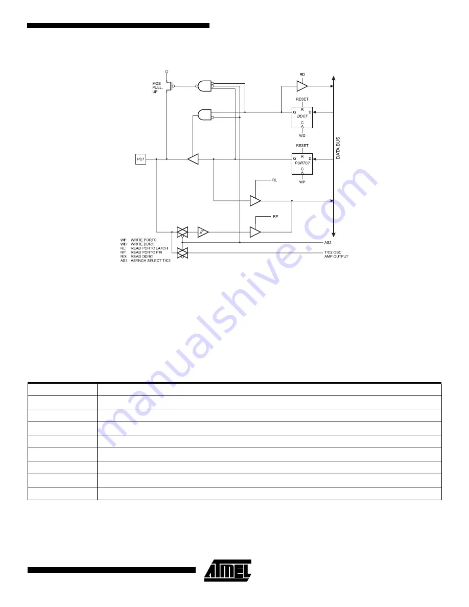
Figure 60.  

Port C Schematic Diagram (Pins PC7)

Port D

Port D is an 8-bit bi-directional I/O port with internal pull-up resistors.

Three I/O memory address locations are allocated for Port D, one each for the Data Register – PORTD, $12($32), Data
Direction Register – DDRD, $11($31) and the Port D Input Pins – PIND, $10($30). The Port D Input Pins address is read-
only, while the Data Register and the Data Direction Register are read/write.

The Port D output buffers can sink 20 mA. As inputs, Port D pins that are externally pulled low will source current if the
pull-up resistors are activated.

Some Port D pins have alternate functions as shown in Table 34.

Table 34.  

Port D Pin Alternate Functions

Port Pin

Alternate Function

PD0

RXD (UART Input line)

PD1

TXD (UART Output line)

PD2

INT0 (External interrupt 0 input)

PD3

INT1 (External interrupt 1 input)

PD4

OC1B (Timer/Counter1 output compareB match output)

PD5

OC1A (Timer/Counter1 output compareA match output)

PD6

ICP (Timer/Counter1 input capture pin)

PD7

OC2 (Timer/Counter2 output compare match output)

Содержание AVR AT90LS4434

Страница 1: ...imer Counter with Separate Prescaler Compare and Capture Modes and Dual 8 9 or 10 bit PWM Programmable Watchdog Timer with On chip Oscillator On chip Analog Comparator Special Microcontroller Features...

Страница 2: ...AL OSCILLATOR WATCHDOG TIMER STACK POINTER PROGRAM FLASH MCU CONTROL REGISTER SRAM GENERAL PURPOSE REGISTERS INSTRUCTION REGISTER TIMER COUNTERS INSTRUCTION DECODER DATA DIR REG PORTB DATA DIR REG POR...

Страница 3: ...SC CPU with In System Programmable Flash on a monolithic chip the Atmel AT90S4434 8535 is a powerful microcontroller that provides a highly flexible and cost effective solution to many embedded contro...

Страница 4: ...es of the AT90S4434 8535 as listed on page 79 The Port D pins are tri stated when a reset condition becomes active even if the clock is not running RESET Reset input An external reset is generated by...

Страница 5: ...gure External Clock To drive the device from an external clock source XTAL2 should be left unconnected while XTAL1 is driven as shown in Figure 3 Figure 3 External Clock Drive Configuration Timer Osci...

Страница 6: ...hitecture The ALU supports arithmetic and logic functions between registers or between a constant and a register Single register operations are also executed in the ALU Figure 4 shows the AT90S4434 85...

Страница 7: ...is effec tively allocated in the general data SRAM and consequently the stack size is only limited by the total SRAM size and the usage of the SRAM All user programs must initialize the SP in the rese...

Страница 8: ...Data Space Although not being physically implemented as SRAM locations this memory organization provides great flexibility in access of the registers as the X Y and Z registers can be set to index any...

Страница 9: ...ding See page 10 for the different program memory addressing modes SRAM Data Memory Figure 8 shows how the AT90S4434 8535 SRAM memory is organized Figure 8 SRAM Organization The lower 352 608 data mem...

Страница 10: ...535 AVR RISC microcontroller supports powerful and efficient addressing modes for access to the pro gram memory Flash and data memory SRAM register file and I O memory This section describes the diffe...

Страница 11: ...data address is contained in the 16 LSBs of a 2 word instruction Rd Rr specify the destination or source register Data Indirect with Displacement Figure 13 Data Indirect with Displacement Operand addr...

Страница 12: ...ore the operation Operand address is the decremented contents of the X Y or the Z register Data Indirect with Post increment Figure 16 Data Indirect Addressing with Post increment The X Y or the Z reg...

Страница 13: ...the Z register contents The 15 MSBs select word address 0 2K 4K the LSB selects low byte if cleared LSB 0 or high byte if set LSB 1 Indirect Program Addressing IJMP and ICALL Figure 18 Indirect Progra...

Страница 14: ...instruction execution and internal memory access The AVR CPU is driven by the System Clock directly generated from the external clock crystal for the chip No internal clock division is used Figure 20...

Страница 15: ...is performed in two System Clock cycles as described in Figure 22 Figure 22 On chip Data SRAM Access Cycles System Clock Total Execution Time Register Operands Fetch ALU Operation Execute Result Writ...

Страница 16: ...Counter1 High Byte 2C 4C TCNT1L Timer Counter1 Low Byte 2B 4B OCR1AH Timer Counter1 Output Compare Register A High Byte 2A 4A OCR1AL Timer Counter1 Output Compare Register A Low Byte 29 49 OCR1BH Tim...

Страница 17: ...itten Some of the status flags are cleared by writing a logical 1 to them Note that the CBI and SBI instructions will operate on all bits in the I O register writing a 1 back into any flag read as set...

Страница 18: ...struc tion Set description for detailed information Bit 3 V Two s Complement Overflow Flag The two s complement overflow flag V supports two s complement arithmetics See the Instruction Set descriptio...

Страница 19: ...with the I bit in the Status Register in order to enable the interrupt The lowest addresses in the program memory space are automatically defined as the Reset and Interrupt vectors The complete list o...

Страница 20: ...MP Analog Comparator Handler 011 MAIN ldi r16 high RAMEND Main program start 012 out SPH r16 013 ldi r16 low RAMEND 014 out SPL r16 015 instr xxx Reset Sources The AT90S4434 8535 has three sources of...

Страница 21: ...l Characteristics on page 100 If the built in start up delay is sufficient RESET can be connected to VCC directly or via an external pull up resistor By hold ing the pin low for a period after VCC has...

Страница 22: ...nger than 50 ns will generate a reset even if the clock is not running Shorter pulses are not guaranteed to generate a reset When the applied signal reaches the Reset Threshold Voltage VRST on its pos...

Страница 23: ...t by writing a logical 1 to the bit Bit 0 PORF Power on Reset Flag This bit is only set by a Power on Reset A Watchdog Reset or an External Reset will leave this bit unchanged The bit is reset by writ...

Страница 24: ...d when returning from an interrupt routine This must be handled by software General Interrupt Mask Register GIMSK Bit 7 INT1 External Interrupt Request 1 Enable When the INT1 bit is set one and the I...

Страница 25: ...nter2 occurs i e when the OCF2 bit is set in the Timer Counter Interrupt Flag Register TIFR Bit 6 TOIE2 Timer Counter2 Overflow Interrupt Enable When the TOIE2 bit is set one and the I bit in the Stat...

Страница 26: ...nput capture event indicating that the Timer Counter1 value has been transferred to the Input Capture Register ICR1 ICF1 is cleared by hardware when executing the corresponding interrupt handling vect...

Страница 27: ...ram Counter 2 bytes is pushed onto the stack and the Stack Pointer is decremented by 2 The vector is normally a relative jump to the interrupt routine and this jump takes two clock cycles If an interr...

Страница 28: ...any of the three sleep modes the SE bit in MCUCR must be set one and a SLEEP instruction must be executed The SM0 and SM1 bits in the MCUCR register select which sleep mode Idle Power down or Power Sa...

Страница 29: ...kes the MCU enter the Power Save Mode This mode is identical to Power down with one exception If Timer Counter2 is clocked asynchronously i e the AS2 bit in ASSR is set Timer Counter2 will run during...

Страница 30: ...as its own prescaler These Timer Counters can either be used as a timer with an internal clock time base or as a counter with an external pin connec tion that triggers the counting Timer Counter Presc...

Страница 31: ...CCR0 The overflow status flag is found in the Timer Counter Interrupt Flag Register TIFR Control signals are found in the Timer Counter0 Control Register TCCR0 The interrupt enable disable settings fo...

Страница 32: ...ntrol Register cleared to zero gives an input pin Timer Counter 0 TCNT0 The Timer Counter0 is realized as an up counter with read and write access If the Timer Counter0 is written and a clock source i...

Страница 33: ...be compared to the Timer Counter1 contents The Output Compare functions include optional clearing of the counter on compareA match and actions on the Output Compare pins on both compare matches Timer...

Страница 34: ...s affect pin OC1B Output CompareB This is an alternative function to an I O port and the corre sponding direction control bit must be set one to control an output pin The control configuration is give...

Страница 35: ...Bit 3 CTC1 Clear Timer Counter1 on Compare Match When the CTC1 control bit is set one the Timer Counter1 is reset to 0000 in the clock cycle after a compareA match If the CTC1 control bit is cleared...

Страница 36: ...is combined with the byte data in the TEMP register and all 16 bits are written to the TCNT1 Timer Counter1 register simultaneously Consequently the high byte TCNT1H must be accessed first for a full...

Страница 37: ...is also used when accessing TCNT1 and ICR1 If the main program and interrupt routines perform access to registers using TEMP interrupts must be disabled during access from the main program Timer Count...

Страница 38: ...etails Note that if the Compare Register contains the TOP value and the prescaler is not in use CS12 CS10 001 the PWM output will not produce any pulse at all because the up counting and down counting...

Страница 39: ...hown in Table 17 Note X A In PWM mode the Timer Overflow Flag1 TOV1 is set when the counter advances from 0000 Timer Overflow Interrupt1 operates exactly as in normal Timer Counter mode i e it is exec...

Страница 40: ...ompare function using the Output Compare Register OCR2 as the data source to be compared to the Timer Counter contents The Output Compare function includes optional clearing of the counter on compare...

Страница 41: ...ck cycle after a compare match If the control bit is cleared Timer Counter2 continues counting and is unaffected by a compare match Since the compare match is detected in the CPU clock cycle following...

Страница 42: ...h A compare match will set the compare interrupt flag in the CPU clock cycle following the compare event Timer Counter2 in PWM Mode When the PWM mode is selected Timer Counter2 and the Output Compare...

Страница 43: ...mode the Timer Overflow Flag TOV2 is set when the counter advances from 00 Timer Overflow Interrupt2 operates exactly as in normal Timer Counter mode i e it is executed when TOV2 is set provided that...

Страница 44: ...nintentional interrupt to occur The mechanisms for reading TCNT2 OCR2 and TCCR2 are different When reading TCNT2 the actual timer value is read When reading OCR2 or TCCR2 the value in the temporary st...

Страница 45: ...registers must be considered lost after a wake up from power down due to the unstable clock signal upon start up regardless of whether the oscillator is in use or a clock signal is applied to the TOSC...

Страница 46: ...on is disabled WDE can only be cleared if the WDTOE bit is set one To disable an enabled Watchdog Timer the following procedure must be followed 1 In the same operation write a logical 1 to WDTOE and...

Страница 47: ...ut reset the Watchdog Timer may not start to count from zero To avoid unintentional MCU resets the Watchdog Timer should be disabled or reset before changing the Watchdog Timer Prescale Select Table 2...

Страница 48: ...e EEPROM read operation the EEDR contains the data read out from the EEPROM at the address given by EEAR EEPROM Control Register EECR Bit 7 4 Res Reserved Bits These bits are reserved bits in the AT90...

Страница 49: ...bit is cleared zero by hardware requested data is found in the EEDR register The EEPROM read access takes one instruction and there is no need to poll the EERE bit When EERE has been set the CPU is ha...

Страница 50: ...output in the Master Mode and is the clock input in the Slave Mode Writing to the SPI Data Register of the master CPU starts the SPI clock generator and the data written shifts out of the PB5 MOSI pin...

Страница 51: ...he following actions 1 The MSTR bit in SPCR is cleared and the SPI system becomes a slave As a result of the SPI becoming a slave the MOSI and SCK pins become inputs 2 The SPIF flag in SPSR is set and...

Страница 52: ...er SPI Mode when set one and Slave SPI Mode when cleared zero If SS is configured as an input and is driven low while MSTR is set MSTR will be cleared and SPIF in SPSR will become set The user will th...

Страница 53: ...Register SPDR is written during a data transfer The WCOL bit and the SPIF bit are cleared zero by first reading the SPI Status Register with WCOL set one and then accessing the SPI Data Register Bit...

Страница 54: ...gure 41 Figure 41 UART Transmitter Data transmission is initiated by writing the data to be transmitted to the UART I O Data Register UDR Data is transferred from UDR to the Transmit shift register wh...

Страница 55: ...ta has been written and the stop bit has been present on TXD for one bit length the TX Complete flag TXC in USR is set The TXEN bit in UCR enables the UART Transmitter when set one When this bit is cl...

Страница 56: ...ontrol Register UCR is set the RXB8 bit in UCR is loaded with bit 9 in the Transmit Shift register when data is transferred to UDR If after having received a character the UDR register has not been re...

Страница 57: ...the corresponding interrupt handling vector Alternatively the TXC bit is cleared zero by writing a logical 1 to the bit Bit 5 UDRE UART Data Register Empty This bit is set one when a character written...

Страница 58: ...shift register plus any following character in UDR has been com pletely transmitted Bit 2 CHR9 9 Bit Characters When this bit is set one transmitted and received characters are 9 bits long plus start...

Страница 59: ...ud Rate 3 2768 MHz Error 3 6864 MHz Error 4 MHz Error 4 608 MHz Error 2400 UBRR 84 0 4 UBRR 95 0 0 UBRR 103 0 2 UBRR 119 0 0 4800 UBRR 42 0 8 UBRR 47 0 0 UBRR 51 0 2 UBRR 59 0 0 9600 UBRR 20 1 6 UBRR...

Страница 60: ...s bit is a reserved bit in the AT90S4434 8535 and will always read as zero Bit 5 ACO Analog Comparator Output ACO is directly connected to the comparator output Bit 4 ACI Analog Comparator Interrupt F...

Страница 61: ...s Conversion Time Up to 15 kSPS at Maximum Resolution 8 Multiplexed Input Channels Rail to rail Input Range Free Running or Single Conversion Mode Interrupt on ADC Conversion Complete Sleep Mode Nois...

Страница 62: ...high as long as the conversion is in progress and will be set to zero by hardware when the conversion is completed If a different data channel is selected while a conversion is in progress the ADC wi...

Страница 63: ...ADC clock cycle A normal conversion takes 13 ADC clock cycles In certain situations the ADC needs more clock cycles for initialization and to minimize offset errors Extended conversions take 25 ADC c...

Страница 64: ...18 19 20 21 22 23 24 25 1 2 Extended Conversion Next Conversion 3 MUX and REFS update MUX and REFS update Conversion complete 1 2 3 4 5 6 7 8 9 10 11 12 13 Sign and MSB of result LSB of result ADC clo...

Страница 65: ...ADC Multiplexer Select Register ADMUX Bits 7 3 Res Reserved Bits These bits are reserved bits in the AT90S4434 8535 and always read as zero Bits 2 0 MUX2 MUX0 Analog Channel Select Bits 2 0 The value...

Страница 66: ...one the ADC operates in Free Running Mode In this mode the ADC samples and updates the data registers continuously Clearing this bit zero will terminate Free Running Mode Bit 4 ADIF ADC Interrupt Flag...

Страница 67: ...conversion has already started and the old setting is used ADC Noise Canceling Techniques Digital circuitry inside and outside the AT90S4434 8535 generates EMI that might affect the accuracy of analo...

Страница 68: ...S8535 68 Figure 50 ADC Power Connections GND VCC PA0 ADC0 PA1 ADC1 PA2 ADC2 PA3 ADC3 PA4 ADC4 PA5 ADC5 PA6 ADC6 PA7 ADC7 AREF AVCC AGND PC0 100nF Analog Ground Plane AT90S4434 8535 39 35 37 33 32 38 3...

Страница 69: ...n pins PA0 to PA7 are used as inputs and are externally pulled low they will source current if the internal pull up resistors are activated Port A has an alternate function as analog inputs for the AD...

Страница 70: ...ll up resistor is activated To switch the pull up resistor off the PORTAn has to be cleared zero or the pin has to be configured as an output pin The port pins are tri stated when a reset condition be...

Страница 71: ...can sink 20 mA and thus drive LED dis plays directly When pins PB0 to PB7 are used as inputs and are externally pulled low they will source current if the internal pull up resistors are activated The...

Страница 72: ...when a reset condition becomes active even if the clock is not running Note n 7 6 0 pin number Alternate Functions of Port B The alternate pin configuration is as follows SCK Port B Bit 7 SCK Master c...

Страница 73: ...e data direc tion of this pin is controlled by DDB4 When the pin is forced to be an input the pull up can still be controlled by the PORTB4 bit See the description of the SPI port for further details...

Страница 74: ...ver not shown in the figures Figure 52 Port B Schematic Diagram Pins PB0 and PB1 Figure 53 Port B Schematic Diagram Pins PB2 and PB3 2 DATA BUS D D Q Q RESET RESET C C WD WP RD MOS PULL UP PBn AINm TO...

Страница 75: ...SS MSTR SPE WP WD RL RP RD MSTR SPE WRITE PORTB WRITE DDRB READ PORTB LATCH READ PORTB PIN READ DDRB SPI MASTER ENABLE SPI ENABLE DDB4 PORTB4 RL RP DATA BUS D D Q Q RESET RESET C C WD WP RD MOS PULL...

Страница 76: ...RP RD SPE MSTR WRITE PORTB WRITE DDRB READ PORTB LATCH READ PORTB PIN READ DDRB SPI ENABLE MASTER SELECT DDB6 PORTB6 SPE MSTR SPI SLAVE OUT SPI MASTER IN RL RP DATA BUS D D Q Q RESET RESET C C WD WP R...

Страница 77: ...DDCn is set one PCn is con figured as an output pin If DDCn is cleared zero PCn is configured as an input pin If PORTCn is set one when the pin is configured as an input pin the MOS pull up resistor i...

Страница 78: ...59 Port C Schematic Diagram Pins PC6 DATA BUS D D Q Q RESET RESET C C WD WP RD MOS PULL UP PCn R R WP WD RL RP RD n WRITE PORTC WRITE DDRC READ PORTC LATCH READ PORTC PIN READ DDRC 0 5 DDCn PORTCn RL...

Страница 79: ...egister are read write The Port D output buffers can sink 20 mA As inputs Port D pins that are externally pulled low will source current if the pull up resistors are activated Some Port D pins have al...

Страница 80: ...e the timer descrip tion on how to enable this function The OC2 pin is also the output pin for the PWM mode timer function ICP Port D Bit 6 ICP Input Capture Pin The PD6 pin can act as an input captur...

Страница 81: ...See the interrupt description for further details and how to enable the source TXD Port D Bit 1 Transmit Data data output pin for the UART When the UART Transmitter is enabled this pin is configured a...

Страница 82: ...D1 Figure 63 Port D Schematic Diagram Pins PD2 and PD3 DATA BUS D D Q Q RESET RESET C C WD WP RD RP RL MOS PULL UP PD1 R R WP WD RL RP RD TXD TXEN WRITE PORTD WRITE DDRD READ PORTD LATCH READ PORTD PI...

Страница 83: ...ort D Schematic Diagram Pin PD6 DATA BUS D D Q Q RESET RESET C C WD WP RD MOS PULL UP PD6 R R WP WD RL RP RD ACIC ACO WRITE PORTD WRITE DDRD READ PORTD LATCH READ PORTD PIN READ DDRD COMPARATOR IC ENA...

Страница 84: ...AT90S LS4434 and AT90S LS8535 84 Figure 66 Port D Schematic Diagram Pin PD7...

Страница 85: ...2 indicates 4K bytes Flash memory 3 002 02 indicates AT90S4434 device when signature byte 001 is 92 For the AT90S8535 1 they are 1 000 1E indicates manufactured by Atmel 2 001 93 indicates 8K bytes Fl...

Страница 86: ...y signal names describing their function during parallel programming See Figure 67 and Table 38 Pins not described in Table 38 are referenced by pin name The XA1 XA0 pins determine the action executed...

Страница 87: ...I Output Enable Active low WR PD3 I Write Pulse Active low BS PD4 I Byte Select 0 selects low byte 1 selects high byte XA0 PD5 I XTAL Action Bit 0 XA1 PD6 I XTAL Action Bit 1 DATA PB7 0 I O Bi direct...

Страница 88: ...te Flash 4 Give XTAL1 a positive pulse This loads the command B Load Address High Byte 1 Set XA1 XA0 to 00 This enables address loading 2 Set BS to 1 This selects high byte 3 Set DATA Address high byt...

Страница 89: ...The command needs only be loaded once when writing or reading multiple memory locations Address high byte needs only be loaded before programming a new 256 word page in the Flash Skip writing the dat...

Страница 90: ...Byte 00 FF 5 E Write Data Low Byte Reading the EEPROM The algorithm for reading the EEPROM memory is as follows refer to Programming the Flash for details on command and address loading 1 A Load Comm...

Страница 91: ...hm for reading the Fuse and Lock bits is as follows refer to Programming the Flash on page 88 for details on command loading 1 A Load Command 0000 0100 2 Set OE to 0 and BS to 1 The status of the Fuse...

Страница 92: ...tXHXL XTAL1 Pulse Width High 67 0 ns tXLDX Data and Control Hold after XTAL1 Low 67 0 ns tXLWL XTAL1 Low to WR Low 67 0 ns tBVWL BS Valid to WR Low 67 0 ns tRHBX BS Hold after RDY BSY High 67 0 ns tWL...

Страница 93: ...dge of SCK When reading data from the AT90S4434 AT90S8535 data is clocked on the falling edge of SCK See Figure 72 Figure 73 and Table 44 for timing details To program and verify the AT90S4434 AT90S85...

Страница 94: ...hed and then the value P2 See Table 42 for P1 and P2 values At the time the device is ready for a new EEPROM byte the programmed value will read correctly This is used to deter mine when the next byte...

Страница 95: ...oooo Read H high or low data o from program memory at word address a b Write Program Memory 0100 H000 xxxx aaaa bbbb bbbb iiii iiii Write H high or low data i to program memory at word address a b Re...

Страница 96: ...C 4 0 6 0V 0 8 0 MHz tCLCL Oscillator Period VCC 4 0 6 0V 125 0 ns tSHSL SCK Pulse Width High 2 0 tCLCL ns tSLSH SCK Pulse Width Low 2 0 tCLCL ns tOVSH MOSI Setup to SCK High tCLCL ns tSHOX MOSI Hold...

Страница 97: ...Current VCC and GND TQFP PLCC package 400 0 mA DC Characteristics TA 40 C to 85 C VCC 2 7V to 6 0V unless otherwise noted Symbol Parameter Condition Min Typ Max Units VIL Input Low Voltage 0 5 0 3VCC...

Страница 98: ...est condition 4 Although each I O port can source more than the test conditions 3 mA at VCC 5V 1 5 mA at VCC 3V under steady state conditions non transient the following must be observed PDIP Package...

Страница 99: ...47 External Clock Drive Symbol Parameter VCC 2 7V to 6 0V VCC 4 0V to 6 0V Units Min Max Min Max 1 tCLCL Oscillator Frequency 0 4 0 8 0 MHz tCLCL Clock Period 250 0 125 0 ns tCHCX High Time 100 0 50 0...

Страница 100: ...re operating voltage and frequency The current drawn from capacitive loaded pins may be estimated for one pin as CL VCC f where CL load capacitance VCC operating voltage and f average switching freque...

Страница 101: ...8 10 12 14 16 2 2 5 3 3 5 4 4 5 5 5 5 6 ACTIVE SUPPLY CURRENT vs Vcc FREQUENCY 4 MHz I cc mA Vcc V T 85 C A T 25 C A 0 2 4 6 8 10 12 14 16 18 20 0 1 2 3 4 5 6 7 8 9 10 11 12 13 14 15 Vcc 6V Vcc 5 5V...

Страница 102: ...ply Current vs VCC 0 1 2 3 4 5 6 7 2 2 5 3 3 5 4 4 5 5 5 5 6 T 25 C A T 85 C A IDLE SUPPLY CURRENT vs Vcc I cc mA Vcc V FREQUENCY 4 MHz 0 10 20 30 40 50 60 70 80 90 2 2 5 3 3 5 4 4 5 5 5 5 6 T 85 C A...

Страница 103: ...upply Current vs VCC 0 20 40 60 80 100 120 140 2 2 5 3 3 5 4 4 5 5 5 5 6 T 85 C A T 25 C A POWER DOWN SUPPLY CURRENT vs Vcc I cc Vcc V WATCHDOG TIMER ENABLED 0 10 20 30 40 50 60 70 80 90 2 2 5 3 3 5 4...

Страница 104: ...g Comparator Offset Voltage vs Common Mode Voltage 0 0 1 0 2 0 3 0 4 0 5 0 6 0 7 0 8 0 9 1 2 2 5 3 3 5 4 4 5 5 5 5 6 ANALOG COMPARATOR CURRENT vs Vcc I cc mA Vcc V T 25 C A T 85 C A 0 2 4 6 8 10 12 14...

Страница 105: ...tor Input Leakage Current 0 2 4 6 8 10 0 0 5 1 1 5 2 2 5 3 ANALOG COMPARATOR OFFSET VOLTAGE vs COMMON MODE VOLTAGE Common Mode Voltage V Offset Voltage mV V 2 7V cc T 85 C A T 25 C A 60 50 40 30 20 10...

Страница 106: ...n one pin at a time Figure 87 Pull up Resistor Current vs Input Voltage 0 200 400 600 800 1000 1200 1400 1600 2 2 5 3 3 5 4 4 5 5 5 5 6 T 85 C A T 25 C A WATCHDOG OSCILLATOR FREQUENCY vs Vcc V V cc F...

Страница 107: ...89 I O Pin Sink Current vs Output Voltage 0 5 10 15 20 25 30 0 0 5 1 1 5 2 2 5 3 PULL UP RESISTOR CURRENT vs INPUT VOLTAGE I A OP V V OP V 2 7V cc T 85 C A T 25 C A 0 10 20 30 40 50 60 70 80 0 0 5 1...

Страница 108: ...I O Pin Sink Current vs Output Voltage 0 2 4 6 8 10 12 14 16 18 0 0 5 1 1 5 2 2 5 3 3 5 4 4 5 5 I O PIN SOURCE CURRENT vs OUTPUT VOLTAGE V 5V cc I mA OH V V OH T 85 C A T 25 C A 0 5 10 15 20 25 30 0...

Страница 109: ...Voltage Figure 93 I O Pin Input Threshold Voltage vs VCC 0 1 2 3 4 5 6 0 0 5 1 1 5 2 2 5 3 I O PIN SOURCE CURRENT vs OUTPUT VOLTAGE I mA OH V V OH T 85 C A T 25 C A V 2 7V cc 0 0 5 1 1 5 2 2 5 2 7 4 0...

Страница 110: ...AT90S LS4434 and AT90S LS8535 110 Figure 94 I O Pin Input Hysteresis vs VCC 0 0 02 0 04 0 06 0 08 0 1 0 12 0 14 0 16 0 18 2 7 4 0 5 0 Input hysteresis V Vcc I O PIN INPUT HYSTERESIS vs Vcc T 25 C A...

Страница 111: ...ounter1 Input Capture Register Low Byte page 37 25 45 TCCR2 PWM2 COM21 COM20 CTC2 CS22 CS21 CS20 page 41 24 44 TCNT2 Timer Counter2 8 Bits page 42 23 43 OCR2 Timer Counter2 Output Compare Register pag...

Страница 112: ...Rd K Compare Register with Immediate Rd K Z N V C H 1 SBRC Rr b Skip if Bit in Register Cleared if Rr b 0 PC PC 2 or 3 None 1 2 3 SBRS Rr b Skip if Bit in Register is Set if Rr b 1 PC PC 2 or 3 None 1...

Страница 113: ...STACK None 2 BIT AND BIT TEST INSTRUCTIONS SBI P b Set Bit in I O Register I O P b 1 None 2 CBI P b Clear Bit in I O Register I O P b 0 None 2 LSL Rd Logical Shift Left Rd n 1 Rd n Rd 0 0 Z C N V 1 LS...

Страница 114: ...I AT90S4434 8JI AT90S4434 8PI 44A 44J 40P6 Industrial 40 C to 85 C 2 7 6 0V 4 AT90LS8535 4AC AT90LS8535 4JC AT90LS8535 4PC 44A 44J 40P6 Commercial 0 C to 70 C AT90LS8535 4AI AT90LS8535 4JI AT90LS8535...

Страница 115: ...26 660 050 1 27 TYP 022 559 X 45 MAX 3X 656 16 7 650 16 5 695 17 7 685 17 4 SQ SQ 2 07 52 6 2 04 51 8 PIN 1 566 14 4 530 13 5 090 2 29 MAX 005 127 MIN 065 1 65 015 381 022 559 014 356 065 1 65 041 1 0...

Страница 116: ...x 41 Casa Postale 80 CH 1705 Fribourg Switzerland TEL 41 26 426 5555 FAX 41 26 426 5500 Asia Atmel Asia Ltd Room 1219 Chinachem Golden Plaza 77 Mody Road Tsimhatsui East Kowloon Hong Kong TEL 852 2721...

Отзывы: