


MODULE CONFIGURATIONS
6.3.2 Configurable RT Response Time
The RT response time of MIL-STD-1553 OmniBus modules may be individually
set in software for each 1553 channel. The response time is measured from the
mid-bit zero crossing of the parity bit to the mid-bit zero crossing of the status
word. The RT response time may be set through software using the
BTI1553_RTResponseTimeSet function. The response time value is an integer
that represents the response time in hundreds of nanoseconds up to 25.5 micro-
seconds. The minimum response time is affected by the error checking process
and is about 3.7 microseconds for MIL-STD-1553A and 7.7 microseconds for
MIL-STD-1553B (the default protocol in BTI1553_RTConfig). Any value below
the minimum yields the minimum. The default RT response time for OmniBus
modules is approximately 9 microseconds (a value of 90). The exact response
time depends on several factors, such as where on the bus it is measured, analog
and digital delays in the on-board circuits, and uncertainty due to the 100-
nanosecond sampling time.
6.3.3 Variable Transmit Amplitude
For OmniBus II MIL-STD-1553 level P channels, the amplitude of the
transmitted databus signal can be varied under software control. Using
BTI1553_ParamAmplitudeConfig, the OmniBus II has extended functionality
from the OmniBus Family. The configuration value, configval, now allows for
setting a high and a low range. The lower 12 bits of dacval represent the transmit
amplitude. The OmniBus II has a resolution of 8 bits, so the least significant 4
bits are “don’t cares.” The full-scale value of FF0h is the default setting.
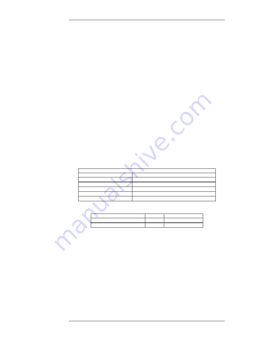
configval
Constant
Description
PARAMCFG1553_DEFAULT
Select all default settings (
bold
below)
PARAMCFG1553_AMPLON
Enables parametric amplitude control
PARAMCFG1553_AMPLHI
Enables parametric amplitude control high range
PARAMCFG1553_AMPLLO
Enables parametric amplitude control low range
PARAMCFG1553_AMPLOFF
Disables parametric amplitude control
Table 6.5—MIL-STD-1553 ParamAmplitudeConfig Configval
Constant
Range*
Output Drive*
PARAMCFG1553_AMPLHI
0V-26V
.101*(dacval >> 4)
PARAMCFG1553_AMPLLO
0V-4.9V .019*(dacval >> 4)
Table 6.6—MIL-STD-1553 ParamAmplitudeConfig Output Drive
*Since the actual amplitude and linearity depend on both the line driver and load,
the user must calibrate with the conditions in use for the degree of accuracy
desired. Some line drivers are not capable of putting out very low voltages; be
sure to verify the output under your operating conditions.
6.3.4 Zero Crossing Distortion
On level P channels, a zero crossing of the transmitted signal can be shifted from
its normal position under software control. This feature allows a specific zero
crossing to be shifted up to plus or minus 250 nanoseconds, in increments of 5
ns. A zero crossing shift can be generated on the leading or mid-bit zero crossing
of a specified bit position in a specified word.
OmniBus II PCIe/PXIe User’s Manual
6-3
Содержание OmniBusII
Страница 2: ......
Страница 4: ......
Страница 8: ...TABLE OF CONTENTS This page intentionally blank iv OmniBus II PCI PXIe User s Manual...
Страница 14: ...INTRODUCTION This page intentionally blank 1 6 OmniBus II PCIe PXIe User s Manual...
Страница 18: ...INSTALLATION This page intentionally blank 2 4 OmniBus II PCIe PXIe User s Manual...
Страница 28: ...OMNIBUS II FEATURES This page intentionally blank 4 8 OmniBus II PCIe PXIe User s Manual...
Страница 34: ...OMNIBUS II PXIE SPECIFIC FEATURES This page intentionally blank 5 6 OmniBus II PCIe PXIe User s Manual...
Страница 42: ...MODULE CONFIGURATIONS This page intentionally blank 6 8 OmniBus II PCIe PXIe User s Manual...
Страница 56: ...COUPLING AND TERMINATION This page intentionally blank A 4 OmniBus II PCIe PXIe User s Manual...
Страница 58: ...REVISION HISTORY This page intentionally blank B 2 OmniBus II PCIe PXIe User s Manual...