CYC1000 User Guide
www.arrow.com
Page | 44
January 2020
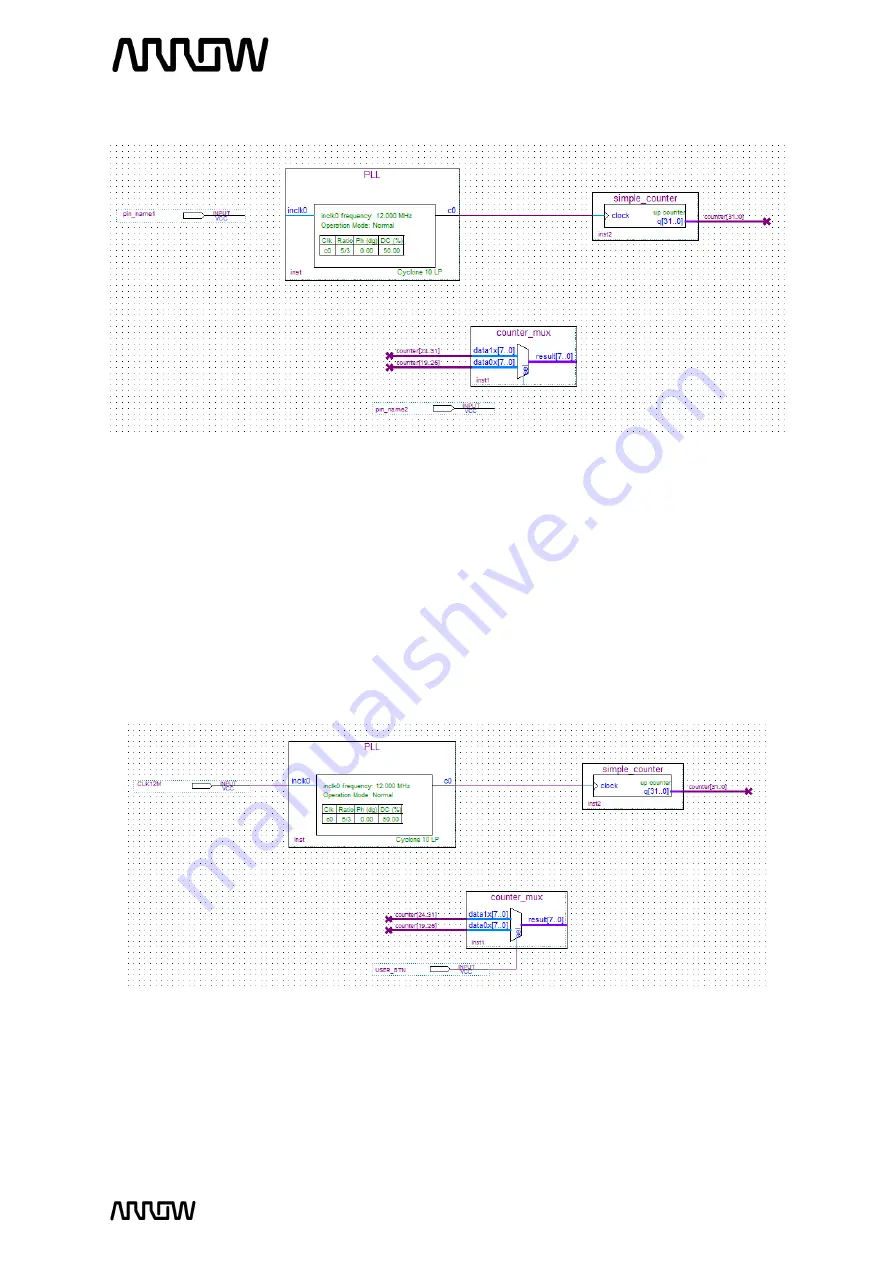
Your schematic should look like this:
5.2.10.3
Rename the pin_name1 to
CLK12M
by double clicking its current name. This is going to
be the clock signal coming into the FPGA.
5.2.10.4
Rename the pin_name2 to
USER_BTN
by double clicking its current name. This is going
to be the user button of the CYC1000 board to select the mux.
5.2.10.5
Using the
“
Node Tool
”
connect:
CLK12M
→
inclk0
(of the PLL component)
USER_BTN
→
sel
(of the counter_mux component)
Your schematic should look like this now:


