background image

2-29

2.4.21.


SET - Set Configuration

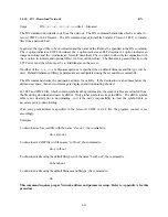
SET

Usage:

SET option <value>
SET

The SET command allows the setting of user configurable options within dBUG.  The options are listed
below.  If the SET command is issued without option,  it will show the available options and values.

The board needs a RESET after this command in order for the new option(s) to take effect.

baud - This is the baud rate for the first serial port on the board.  All communications between dBUG and
the user occur using either 9600 or 19200 bps, eight data bits, no parity, and one stop bit, 8N1. Do not
choose 38400 baud.

base - This is the default radix for use in converting number from their ASCII text representation to the
internal quantity used by dBUG.  The default is hexadecimal (base 16), and other choices are binary (base
2), octal (base 8), and decimal (base 10).

client - This is the network Internet Protocol, IP, address of the board.  For network communications, the
client IP is required to be set to a unique value, usually assigned by your local network administrator.

server - This is the network IP address of the machine which contains files accessible via TFTP.  Your
local network administrator will have this information and can assist in properly configuring a TFTP server
if one does not exist.

gateway - This is the network IP address of the gateway for your local subnetwork.  If the client IP address
and server IP address are not on the same subnetwork, then this option must be properly set.  Your local
network administrator will have this information.

netmask - This is the network address mask to determine if use of a gateway is required.  This field must be
properly set.  Your local network administrator will have this information.

filename - This is the default filename to be used for network download if no name is provided to the DN
command.

filetype - This is the default file type to be used for network download if no type is provided to the DN
command.  Valid values are: “s-record”, “coff”, “image”, and “elf”.

autoboot - This option allows for the automatic downloading and execution of a file from the network.
This option can be used to automatically boot an operating system from the network.  Valid values are:
“on” and “off”.  This option is not implemented on the current of dBUG.

nicbase - this is base address of the network interface.  This command is used 

to inform the dBUG

 of the

address of the network interface. The default value shows 0x0000.  However, this parameter is hard coded
to 0x300.  

DO NOT CHANGE THIS OPTION.

macaddr - This is the ethernet MAC address of the board.  For network communications, the MAC address
is required to be set to a unique value.  Any address that is not already in use is suitable.

Содержание SBC5307

Страница 1: ...SBC5307 USER S MANUAL REVISION 2 0 Copyright 1998 Arnewsh Inc Arnewsh Inc P O Box 270352 Fort Collins CO 80527 0352 Phone 970 223 1616 Fax 970 223 9573 ...

Страница 2: ... directly or indirectly threaten life result in personal injury or cause damage to property Although every effort has been made to make the supplied software and its documentation as accurate and functional as possible Motorola Inc will not assume responsibility for any damages incurred or generated by this product Motorola does not assume any liability arising out of the application or use of any...

Страница 3: ...address below Dated proof of purchase such as a copy of the invoice must be enclosed with the shipment We will return the shipment prepaid via UPS This warranty does not apply if in the opinion of Arnewsh Inc the product has been damaged by accident misuse neglect misapplication or as a result of service or modification other than specified in the manual by others Please send the board and cables ...

Страница 4: ...HAT IS DBUG 2 1 2 2 OPERATIONAL PROCEDURE 2 2 2 2 1 System Power up 2 2 2 2 2 System Initialization 2 4 2 2 2 1 Hard RESET Button 2 4 2 2 2 2 ABORT Button 2 4 2 2 2 3 Software Reset Command 2 4 2 2 2 4 USER Program 2 5 2 2 3 System Operation 2 5 2 3 TERMINAL CONTROL CHARACTERS 2 5 2 4 DBUG COMMAND SET 2 6 2 4 1 AS Assemble AS 2 8 2 4 2 BC Compare Blocks of Memory BC 2 10 2 4 3 BF Block of Memory F...

Страница 5: ...F5307 Registers and Memory Map 3 3 3 1 9 Reset Vector Mapping 3 4 3 1 10 TA Generation 3 4 3 1 11 Wait State Generator 3 4 3 2 THE SDRAM DIMM 3 5 3 3 FLASH ROM 3 5 3 3 1 JP1 Jumper and User s Program 3 5 3 4 THE SERIAL COMMUNICATION CHANNELS 3 5 3 4 1 The MCF5307 DUART 3 6 3 4 2 Motorola Bus M Bus Module 3 6 3 5 THE PARALLEL I O PORT 3 6 3 6 ON BOARD ETHERNET LOGIC 3 7 3 7 THE CONNECTORS AND THE E...

Страница 6: ...THE J7 CONNECTOR PIN ASSIGNMENT 3 10 TABLE 7 THE J8 CONNECTOR PIN ASSIGNMENT 3 10 TABLE 8 THE J9 CONNECTOR PIN ASSIGNMENT 3 11 TABLE 9 THE LA2 CONNECTOR PIN ASSIGNMENT 3 12 TABLE 10 THE LA1 CONNECTOR PIN ASSIGNMENT 3 13 TABLE 11 THE LA3 CONNECTOR PIN ASSIGNMENT 3 13 TABLE 12 THE LA4 CONNECTOR PIN ASSIGNMENT 3 14 TABLE 13 THE LA5 CONNECTOR PIN ASSIGNMENT 3 14 TABLE 14 THE J1 CONNECTOR PIN ASSIGNMEN...

Страница 7: ...RE 1 BLOCK DIAGRAM OF THE BOARD 1 2 FIGURE 2 PIN ASSIGNMENT FOR J4 TERMINAL CONNECTOR 1 6 FIGURE 3 SYSTEM CONFIGURATION 1 7 FIGURE 4 JUMPER AND CONNECTOR PLACEMENT 1 8 FIGURE 5 FLOW DIAGRAM OF DBUG OPERATIONAL MODE 2 3 ...

Страница 8: ...all the built in I O functions of the MCF5307 for learning and evaluating the attributes of the MCF5307 The MCF5307 is a member of the ColdFire family of processors It is a 32 bit processor with 32 bits of addressing and 32 lines of data The processor has eight 32 bit data registers eight 32 bit address registers a 32 bit program counter and a 16 bit status register The MCF5307 has a System Integr...

Страница 9: ...0 U11 ispLSI 2032LV U9 XCEIVERS Flash 1Mbit DRAM DIMM Data Buffers U16 MCF5307 RJ45 Ethernet U12 J3 U20 U21 U23 I O PORTS ADDR BUS DATA BUS CONTROL BUS Mictor and Expansion Connectors Figure 1 Block Diagram of the board ...

Страница 10: ...rminal In addition the signals of both channels are available on the mictor connectors LA1 and LA3 to be viewed by a logic analyzer UART1 channel is the TERMINAL channel used by the debugger for communication with external terminal PC The TERMINAL baud rate is set at 19200 The MCF5307 also incorporate the M Bus which is compatible with I2 C Bus standard The I2 C bus is connected to the DIMM socket...

Страница 11: ...aring the board for the first time be sure to check that all jumpers are in the default locations The standard configuration does not require any modifications After the board is functional in its standard configuration you may use the Ethernet by following the instructions provided in the following sections 1 9 1 Unpacking Unpack the computer board from its shipping box Save the box for storing o...

Страница 12: ...or firmware configures the channel for 19200 baud After the ROM Monitor is running you may issue the SET command to choose any baud rate supported by the ROM Monitor Refer to Chapter 2 for the discussion of this command 1 9 5 The Terminal Character Format The character format of the communication channel is fixed at the power up or RESET The character format is 8 bits per character no parity and o...

Страница 13: ...tion software packages provide a command known as Alt p press the p key while pressing the Alt key to choose the baud rate and character format Make sure you select 8 bits no parity one stop bit see section The Terminal Character Format Then select the baud rate as 19200 Now you are ready to apply power to the board Figure 2 Pin assignment for J4 Terminal connector 1 Data Carrier Detect Output sho...

Страница 14: ...1 7 SBC5307 7 5 to 12V GND Power Supply MICROPROCESSOR EXPANSION BUS BACKGROUND DEBUG BDM Con J4 J7 J8 J9 RS232 TERMINAL or PC dBUG J6 J1 U23 SDRAM D Figure 3 System Configuration ...

Страница 15: ...1 8 J1 J4 J7 J8 J9 JP1 J2 Figure 4 Jumper and connector placement ...

Страница 16: ...u do not get the above response perform the following checks 1 Make sure that the power supply is properly set and connected to the board 2 Check that the terminal and board are set for the same character format and baud 3 Press the black RESET button to insure that the board has been initialized properly If you still are not receiving the proper response your board may have been damaged in shippi...

Страница 17: ...DM simply connect the 26 pin IDC header at the end of the BDM cable provided by the BDM development tool third party tool to the J1 connector No special setting is needed Refer to the BDM User s Manual for additional instructions IMPORTANT There is no key to protect the BDM cable from being rotated and plugged in incorrectly To prevent hooking up the BDM cable incorrectly be careful to notice pin ...

Страница 18: ...Wherever possible dBUG displays data in 80 columns or less dBUG echoes each character as it is typed eliminating the need for any local echo on the terminal side In general dBUG is not case sensitive Commands may be entered either in upper or lower case depending upon the user s equipment and preference Only symbol names require that the exact case be used Most commands can be recognized by using ...

Страница 19: ...s maintained by dBUG These are listed below A0 A7 D0 D7 PC SR All control registers on ColdFire are not readable by the supervisor programming model and thus not accessible via dBUG User code may change these registers but caution must be exercised as changes may render dBUG useless A reference to SP actually refers to A7 2 2 OPERATIONAL PROCEDURE System power up and initial operation are describe...

Страница 20: ...2 3 Figure 5 Flow Diagram of dBUG Operational Mode ...

Страница 21: ...the date xxx 199x xx xx xx may vary in different revisions Other means can be used to re initialize the SBC5307 Computer Board firmware These means are discussed in the following paragraphs 2 2 2 1 Hard RESET Button Hard RESET is the red button located in the lower right side of the board Depressing this button causes all processes to terminate resets the MCF5307 processor and board logic s and re...

Страница 22: ...ress of the memory installed in the board When first learning the system the user should limit his her activities to this area of the memory map Address range 00000000 0001FFFF is used by dBUG 2 If a command causes the system to access an unused address i e no memory or peripheral devices are mapped at that address a bus trap error will occur This results in the terminal printing out a trap error ...

Страница 23: ...ss enter key e CTRL R Recall and execute the last command entered does not need the enter key to be pressed For characters requiring the control key CTRL the CTRL should be pushed and held down and then the other key H should be pressed 2 4 dBUG COMMAND SET Table 3 lists the dBUG commands Each of the individual commands is described in the following pages ...

Страница 24: ...ILL BREAKPOINT GT ADDR 2 20 HELP HELP HELP COMMAND 2 21 IRD INTERNAL REGISTER DISPLAY IRD MODULE REGISTER 2 22 IRM INTERNAL REGISTER MODIFY IRM MODULE REGISTER DATA 2 23 MD MEMORY DISPLAY MD WIDTH BEGIN END 2 24 MM MEMORY MODIFY MM WIDTH ADDR DATA 2 25 RD REGISTER DISPLAY RD REG 2 26 RM REGISTER MODIFY RM REG DATA 2 27 RESET RESET RESET 2 28 SET SET CONFIGURATIONS SET OPTION VALUE 2 29 SHOW SHOW C...

Страница 25: ...S command by inputting a period The inline assembler permits the use of case sensitive symbols defined by equate statements and labels which are stored in the symbol table The syntax for defining symbols and labels is as follows Symbol equ value Symbol equ value Symbol equ value Symbol equ value Label instruction Label Constants and operands may be input in several different bases 0x followed by h...

Страница 26: ...2 9 0x00012002 nop 0x00012004 lsr l 1 d0 0x00012006 cmp 4 d0 0x00012008 beq start 0x0001200A ...

Страница 27: ...ntical then the addresses of the first mismatch are displayed The value for addresses first and second may be an absolute address specified as a hexadecimal value or a symbol name The value for length may be a symbol name or a number converted according to the user defined radix normally hexadecimal Examples To verify that the code in the first block of user FLASH space 128K is identical to the co...

Страница 28: ... normally hexadecimal This command first aligns the starting address for the data access size and then increments the address accordingly during the operation Thus for the duration of the operation this command performs properly aligned memory accesses Examples To fill a memory block starting at 0x00010000 and ending at 0x00040000 with the value 0x1234 the command is bf 10000 40000 1234 To fill a ...

Страница 29: ...and dest may be an absolute address specified as a hexadecimal value or a symbol name If the destination address overlaps the block defined by begin and end an error message is produced and the command exits Examples To copy a block of memory starting at 0x00040000 and ending at 0x00080000 to the location 0x00200000 the command is bm 40000 80000 200000 To copy the target code s data section define...

Страница 30: ...the breakpoint Each time a breakpoint is encountered during the execution of target code the count value is compared against the trigger value If the count value is equal to or greater than the trigger value a breakpoint is encountered and control returned to dBUG By default the initial trigger value for a breakpoint is one but the t option allows setting the initial trigger for the breakpoint If ...

Страница 31: ...properly aligned memory accesses Examples To search for the 16 bit value 0x1234 in the memory block starting at 0x00040000 and ending at 0x00080000 the command is bs 40000 80000 1234 This reads the 16 bit word located at 0x00040000 and compares it against the 16 bit value 0x1234 If no match is found then the address is incremented to 0x00040002 and the next 16 bit value is read and compared To sea...

Страница 32: ...bsolute value If an absolute value passed into the DATA command is prefixed by 0x then data is interpreted as a hexadecimal value Otherwise data is interpreted as a decimal value All values are treated as 32 bit quantities Examples To display the decimal equivalent of 0x1234 the command is data 0x1234 To display the hexadecimal equivalent of 1234 the command is data 1234 ...

Страница 33: ...ol table to produce a more meaningful disassembly This is especially useful for branch target addresses and subroutine calls The DI command attempts to track the address of the last disassembled opcode If no address is provided to the DI command then the DI command uses the address of the last opcode that was disassembled Examples To disassemble code that starts at 0x00040000 the command is di 400...

Страница 34: ...t The DL command checks the destination address for validity If the destination is an address below the defined user space 0x00000000 0x00020000 then an error message is displayed and downloading aborted If the S record file contains the entry point address then the program counter is set to reflect this address Examples To download an S record file through the serial port the command is dl To dow...

Страница 35: ...are manipulated using the set and show commands The DN command checks the destination address for validity If the destination is an address below the defined user space then an error message is displayed and downloading aborted For ELF and COFF files which contain symbolic debug information the symbol tables are extracted from the file during download and used by dBUG Only global symbols are kept ...

Страница 36: ...hen the GO command is executed all user defined breakpoints are inserted into the target code and the context is switched to the target program Control is only regained when the target code encounters a breakpoint illegal instruction or other exception which causes control to be handed back to dBUG Examples To execute code at the current program counter the command is go To execute code at the C f...

Страница 37: ...he GT command executes the target code starting at address in PC whatever the PC has until a temporary breakpoint as given in the command line is reached Example To execute code at the current program counter and stop at breakpoint address 0x10000 the command is GT 10000 ...

Страница 38: ...n If command is provided then a brief listing of the syntax of the specified command is displayed Examples To obtain a listing of all the commands available within dBUG the command is help The help list is longer than one page The help command displays one screen full and ask for an input to display the rest of the list To obtain help on the breakpoint command the command is help br ...

Страница 39: ...e module refers to the module name where the register is located and the register refers to the specific register needed The registers are organized according to the module to which they belong The available modules on the MCF5307 are SIM UART1 UART2 TIMER M Bus DRAMC and Chip Select Refer to MCF5307 User s Manual Example ird sim sypcr display the SYPCR register in the SIM module ...

Страница 40: ...the module name where the register is located register refers to the specific register needed and data is the new value to be written into that register The registers are organized according to the module to which they belong The available modules on the MCF5307 are SIM UART1 UART2 TIMER M Bus DRAMC Chip Select Refer to MCF5307 User s Manual Example irm timer tmr1 0021 write 0021 into TMR1 registe...

Страница 41: ...ng address This command first aligns the starting address for the data access size and then increments the address accordingly during the operation Thus for the duration of the operation this command performs properly aligned memory accesses Examples To display memory at address 0x00400000 the command is md 400000 To display memory in the data section defined by the symbols data_start and data_end...

Страница 42: ...lue for data is provided then the MM command enters into a loop The loop obtains a value for data sets the contents of the current address to data increments the address according to the data size and repeats The loop terminates when an invalid entry for the data value is entered i e a period This command first aligns the starting address for the data access size and then increments the address ac...

Страница 43: ...s the register set of the target If no argument for reg is provided then all registers are displayed Otherwise the value for reg is displayed Examples To display all the registers and their values the command is rd To display only the program counter the command is rd pc ...

Страница 44: ...symbol name or it is converted according to the user defined radix normally hexadecimal dBUG preserves the registers by storing a copy of the register set in a buffer The RM command updates the copy of the register in the buffer The actual value will not be written to the register until target code is executed Examples To change register D0 to contain the value 0x1234 the command is rm D0 1234 ...

Страница 45: ... The RESET command executes the same sequence of code that occurs at power on This code attempts to initialize the devices on the board and dBUG data structures If the RESET command fails to reset the board to your satisfaction cycle power or press the reset button Examples To reset the board and clear the dBUG data structures the command is reset ...

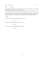
Страница 46: ...er if one does not exist gateway This is the network IP address of the gateway for your local subnetwork If the client IP address and server IP address are not on the same subnetwork then this option must be properly set Your local network administrator will have this information netmask This is the network address mask to determine if use of a gateway is required This field must be properly set Y...

Страница 47: ... choices the command is set To set the baud rate of the board to be 19200 the command is set baud 19200 Now press the RESET button RED or RESET command for the new baud to take effect This baud will be programmed in Flash ROM and will be used during the power up ...

Страница 48: ... options configurable via the SET command can be displayed with the SHOW command If the SHOW command is issued without any option it will show all options Examples To display all the current options the command is show To display the current baud rate of the board the command is show baud To display the TFTP server IP address the command is show server ...

Страница 49: ...he current program counter and then executes the target code The ST command can be used for BSR and JSR instructions The ST command will work for other instructions as well but note that if the ST command is used with an instruction that will not return i e BRA then the temporary breakpoint may never be encountered and thus dBUG may not regain control Examples To pass over a subroutine call the co...

Страница 50: ...lears the entire symbol table the l option lists the contents of the symbol table and the s option displays usage information for the symbol table Symbol names contained in the symbol table are truncated to 31 characters Any symbol table lookups either by the SYMBOL command or by the disassembler will only use the first 31 characters Symbol names are case sensitive Examples To define the symbol ma...

Страница 51: ...e value for num is a decimal number The TRACE command sets bits in the processors supervisor registers to achieve single instruction execution and the target code executed Control returns to dBUG after a single instruction execution of the target code Examples To trace one instruction at the program counter the command is tr To trace 20 instructions from the program counter the command is tr 20 ...

Страница 52: ...hen updates to the MCF5307 EVS dBUG are available the updated image is downloaded to address 0x00020000 The new image is placed into Flash using the UPDBUG command The user is prompted for verification before performing the operation Use this command with extreme caution as any error can render dBUG and thus the board useless ...

Страница 53: ...ser Flash the image is downloaded to address 0x00020000 and the UPUSER command issued This command programs all six sectors of user Flash space Users access this space starting at address 0xFFE20000 To program less than six sectors supply the number of sectors you wish to program after the UPUSER command Examples To program all 6 sectors of user FLASH space the command is upuser or upuser 6 To pro...

Страница 54: ...ven The version number is separated by a decimal for example v1 1 The first number indicates the version of the CPU specific code and the second number indicates the version of the board specific code The version date is the day and time at which the entire dBUG monitor was compiled and built Examples To display the version of the dBUG monitor the command is version ...

Страница 55: ...s the character move l 0013 d0 Selects the function TRAP 15 The character in d1 is sent to terminal C example void board_out_char int ch If your C compiler produces a LINK UNLK pair for this routine then use the following code which takes this into account if l LINK a6 0 produced by C compiler asm move l 8 a6 d1 put ch into d1 asm move l 0x0013 d0 select the function asm trap 15 make the call UNLK...

Страница 56: ...value in D0 means a character is present Assembly example move l 0014 d0 Select the function trap 15 Make the call d0 contains the response yes no C example int board_char_present void asm move l 0x0014 d0 select the function asm trap 15 make the call 2 5 4 EXIT_TO_dBUG This function function code 0x0000 transfers the control back to the dBUG by terminating the user code The register context are p...

Страница 57: ...pace using internal chip select logic All the processor s signals are available through mictor connectors LA1 LA2 LA3 LA4 and LA5 Refer to section 3 7 for pin assignment The MCF5307 has an IEEE JTAG compatible port and BDM port These signals are available at port J1 The processor also has the logic to generate up to eight 8 chip selects CS0 to CS7 and support ADRAM or SDRAM 3 1 2 The Reset Logic T...

Страница 58: ... System Protection Register The dBUG initializes this register with the value 00 which provides for 1024 system clock time out 3 1 6 Interrupt Sources The ColdFire family of processors can receive interrupts for seven levels of interrupt priorities When the processor receives an interrupt which has higher priority than the current interrupt mask in status register it will perform an interrupt ackn...

Страница 59: ... ethernet controller All the I O registers are memory mapped The MCF5307 has built in logic and up to eight chip select pins CS0 to CS7 which are used to enable external memory and I O devices In addition there are two RAS lines for DRAM s There are registers to specify the address range type of access and the method of TA generation for each chip select and RAS pins These registers are programmed...

Страница 60: ...necessary information address R W etc and asserting the TS The processor then waits for an acknowledgment TA by the addressed device before it can complete the bus cycle This TA is used not only to indicate the presence of a device it also allows devices with different access time to communicate with the processor properly The MCF5307 as part of the chip select logic has a built in mechanism to ge...

Страница 61: ...chips The MCF5307 chip select logic can be programmed to generate the TA for CS0 signal after a certain number of wait states The dBUG programs this parameter to three wait states 3 3 1 JP1 Jumper and User s Program This jumper allows users to test code from the boot without having to overwrite the ROM Monitor When the jumper is set between pins 1 and 2 the behavior is normal When the jumper is se...

Страница 62: ...the register map 3 4 2 Motorola Bus M Bus Module The MCF5307 has a built in M Bus module which allows interchip bus interface for a number of I O devices It is compatible with industry standard I 2 C Bus The SBC5307 does not use this module and it is available to the user The two M Bus signals are SDA and SCL which are available at LA4 connector These signals are open collector signals However the...

Страница 63: ...e read byte will be in the lower byte of the read word Below is an example of the data structure used to define the registers For the description of the registers refer to the Data Sheet for Davicom DM9008 a copy of this document in on Coldfire Website typedef struct NATURAL16 CR union struct Even registers NATURAL16 CLDA1 CLDA1 rd PSTOP wr NATURAL16 TSR TSR rd TPSR wr NATURAL16 FIFO FIFO rd TBCR1...

Страница 64: ...ATURAL16 TPSR Transmit Page Start Address rd NATURAL16 ACU Address Counter Upper NATURAL16 reserved0 NATURAL16 reserved2 NATURAL16 RCR Receive Configuration Register rd NATURAL16 DCR Data Configuration Register rd NATURAL16 reserved 0x10000 0x0010 2 Odd registers NATURAL16 PSTART PSTART rd CLDA0 wr NATURAL16 RNPP Remote Next Packet Pointer NATURAL16 LNPP Local Next Packet Pointer NATURAL16 ACL Add...

Страница 65: ...r a PC with terminal emulation software The available signals are a working subset of the RS 232C standard Table 5 The J4 Terminal Connector pin assignment shows the pin assignment Table 5 The J4 Terminal Connector pin assignment PIN NO DIRECTION SIGNAL NAME 1 Output Data Carrier Detect shorted to 4 6 2 Output Receive data 3 Input Transmit data 4 Input Data Terminal Ready shorted to 1 6 5 Signal G...

Страница 66: ... to the data sheets for the major parts and the schematic at the end of this manual to obtain an accurate loading capability A subset of the signals are available on J8 and J9 for easier access Tables 7 14 show the pin assignment for J8 J9 LA1 LA2 LA3 LA4 and LA5 respectively Table 7 The J8 Connector pin assignment PIN NO SIGNAL NAME PIN NO SIGNAL NAME 1 TIN1 2 TT0_PP0 3 TOUT1 4 TT1_PP1 5 TIN0 6 T...

Страница 67: ...1 A3 12 D7 13 A4 14 D8 15 A5 16 D9 17 A6 18 D10 19 A7 20 D11 21 A8 22 D12 23 A9 24 D13 25 A10 26 D14 27 A11 28 D15 29 A12 30 D16 31 A13 32 D17 33 A14 34 D18 35 A15 36 D19 37 A16 38 D20 39 A17 40 D21 41 A18 42 D22 43 A19 44 D23 45 A20 46 D24 47 A21 48 D25 49 A22 50 D26 51 A23 52 D27 53 R W 54 D28 55 AS 56 D29 57 TA 58 D30 59 GND 60 D31 ...

Страница 68: ... 4 A0 5 A1 6 A3 7 A5 8 A7 9 A9 10 A11 11 A13 12 A15 13 A17 14 A19 15 A21 16 A23 17 A25_PP9 18 A27_PP11 19 A29_PP13 20 A31_PP15 21 A30_PP14 22 A28_PP12 23 A26_PP10 24 A24_PP8 25 A22 26 A20 27 A18 28 A16 29 A14 30 A12 31 A10 32 A8 33 A6 34 A4 35 A2 36 NC 37 NC 38 NC 39 GND 40 GND 41 GND 42 GND 43 GND ...

Страница 69: ...5 NC 36 NC 37 NC 38 NC 39 GND 40 GND 41 GND 42 GND 43 GND Table 11 The LA3 Connector pin assignment PIN NO SIGNAL NAME PIN NO SIGNAL NAME 1 NC 2 NC 3 NC 4 PST3 5 PST0 6 PST1 7 PST2 8 DREQ0_PP6 9 DREQ1_PP5 10 MTMOD0 11 MTMOD1 12 RXD2 13 RTS2 14 RXD1 15 MTMOD2 16 DSCLK_ TRST 17 DSDO_TDI 18 TCK 19 BKPT_TMS 20 HIZ 21 DSDO_TDO 22 CTS2 23 CTS1 24 RTSI 25 MTMOD3 26 DDATA0 27 DDATA1 28 DDATA2 29 DDATA3 30...

Страница 70: ...NC 26 NC 27 NC 28 NC 29 NC 30 BWE0 31 BWE3 32 BEW2 33 BWE1 34 TIN1 35 TOUT1 36 NC 37 NC 38 NC 39 GND 40 GND 41 GND 42 GND 43 GND Table 13 The LA5 Connector pin assignment PIN NO SIGNAL NAME PIN NO SIGNAL NAME 1 NC 2 NC 3 NC 4 D1 5 D3 6 D5 7 D7 8 D9 9 D11 10 D13 11 D15 12 D17 13 D19 14 D21 15 D23 16 D25 17 D27 18 D29 19 D31 20 D30 21 D28 22 D26 23 D24 24 D22 25 D20 26 D18 27 D16 28 D14 29 D12 30 D1...

Страница 71: ...J1 Table 14 The J1 Connector pin assignment shows the pin assignment Table 14 The J1 Connector pin assignment PIN NO SIGNAL NAME 1 No Connect 2 BKPT 3 Ground 4 DSCLK 5 Ground 6 No Connect 7 RESET 8 DSI 9 No Connect 10 DSO 11 Ground 12 PST3 13 PST2 14 PST1 15 PST0 16 DDAT3 17 DDAT2 18 DDAT1 19 DDAT0 20 Ground 21 No Connect 22 No Connect 23 Ground 24 CLK 25 3 3 Volts 26 No Connect ...

Страница 72: ...ownload command requires the following three parameters IP address of the TFTP server server IP Name of the file to download filename Type of the file to download filetype of S record COFF ELF or Image Your local system administrator can assign a unique IP address for the board and also provide you the IP addresses of the gateway netmask and TFTP server Fill out the lines below with this informati...

Страница 73: ...ype for network downloads is maintained by dBUG as well To change the default filetype use the command set filetype srecord coff elf image Continuing with the above example the compiler produces an executable COFF file a out This file is copied to the tftp_boot directory on the server with the command rcp a out santafe tftp_boot a out Change the default filename and filetype with the commands set ...

Страница 74: ... to the TFTP server as well Is the default TFTP root directory present and readable If ICMP_DESTINATION_UNREACHABLE or similar ICMP message appears then a serious error has occurred Reset the board and wait one minute for the TFTP server to time out and terminate any open connections Verify that the IP addresses for the server and gateway are correct ...

Страница 75: ...pin 4 Output to ColdFire reset DB_CS_L pin 5 Output Data buffer enable for ethernet A0IN pin 6 INPUT A0 received from CF through buffers IOCHRDY pin 7 Input asserted by ethernet IOCS16L pin 9 Input asserted by ethernet SIZ1 pin 10 XCLK0 pin 11 Input global clock IOWL pin 15 Input write signal from ethernet RD pin 16 INPUT R W from the ColdFire CLK8MHZ pin 17 ISTYPE reg_d buffer BALE pin 18 Output ...

Страница 76: ...erter macro OB21 MACRO XO0 A0 XO0 A0 Tristate Output inverter macro OT21 MACRO XO0 A0 OE XO0 OE OE XO0 A0 CBU43 MACRO Q0 Q1 Q2 CLK EN CS Q0 Q2 clk CLK Q0 D Q0 Q CS EN CS Q1 D Q1 Q CS Q0 Q EN CS Q2 D Q2 Q CS Q0 Q Q1 Q EN CS equations Bidirectional circuit equations OT21 TAL DA DAOE OB21 IORL IOR OB21 IOWL IOW OB21 RST_L RST_H SBHEL 1 IRQ3 ETHER_IRQ DB_CS_L RST_H CS3_L ABORTML ABORTIL ABORTML clk CL...

Страница 77: ...D16 ENDIT IOCS16L RD CLK8MHZ SBHE CS3_L END8 ENDIT RD CLK8MHZ DLYDA CS3_L DA CS3_L DA clk XCLK0 DLYDA CS3_L END16 ENDIT IOCS16L RD CLK8MHZ SBHE CS3_L END8 ENDIT IOCS16L RD CLK8MHZ CS3_L END8 ENDIT SBHE RD CLK8MHZ DLYDA clk XCLK0 STARTISA CS3_L ENDIT STARTISA clk CLK8MHZ CBU43 BCLK0 BCLK1 BCLK2 CLK8MHZ STARTISA STARTISA BALE STARTISA CLK8MHZ BCLK2 BCLK1 BCLK0 IOR IOW IOR STARTISA BCLK2 BCLK1 BCLK0 ...

Страница 78: ... Vector Section test_vectors HIZ_L Test Vector XCLK0 RSTIN_L PORIN_L BDM_RST_L CS3_L RST_H P 1 1 1 1 X C 1 1 1 1 X C 1 0 1 1 X C 1 0 1 1 X C 1 1 1 1 X C 1 1 1 1 X C 0 1 1 1 X C 0 1 1 1 X C 0 1 1 1 X C 1 1 1 1 X C 1 1 0 1 X C 1 1 1 1 X C 1 1 1 1 X C 1 1 1 1 X C 0 1 1 1 X C 0 1 1 1 X C 0 1 1 1 X C 0 1 1 0 X C 0 1 1 0 X C 0 1 1 0 X C 0 1 1 1 X C 0 1 1 1 X C 0 1 1 1 X C 1 1 1 1 X C 1 1 1 1 X C 1 1 1 0...

Страница 79: ...9 APPENDIX C Schematics ...

Страница 80: ...0 192 GND14 101 DDATA2 189 GND15 104 MTMOD1 177 GND16 109 DDATA3 190 GND17 117 TT0 PP0 207 GND18 125 MTMOD2 181 GND19 133 PST1 193 GND20 141 MTMOD3 182 GND21 148 BWE0 96 GND22 156 GND12 85 PST2 195 GND23 162 TT1 PP1 206 GND24 169 PST3 196 GND25 173 IRQ1 72 GND26 178 TM0 PP2 204 GND27 183 BWE1 98 GND28 188 TM1 PP3 203 GND29 194 CS0 50 GND30 201 TM2 PP4 202 GND31 208 BWE2 99 DREQ1 PP5 200 IRQ3 71 DR...

Страница 81: ...IO_1 4 IO_4 34 NC1 1 IO_6 33 IO_3 5 IO_8 32 NC2 2 IO_10 31 IO_5 6 IO_12 30 NC3 37 IO_14 29 IO_7 7 IO_16 28 NC4 38 IO_18 27 IO_9 8 IO_20 26 IO_11 9 IO_22 25 IO_13 10 IO_24 24 IO_15 11 IO_26 23 IO_17 12 IO_28 22 IO_19 13 IO_30 21 IO_21 14 IO_32 20 IO_23 15 IO_25 16 IO_27 17 IO_29 18 IO_31 19 CLK_0_1 3 CLK_0_2 36 G1 39 G2 40 G3 41 G4 42 G5 43 LA2 Mictor_Connector IO_2 35 IO_1 4 IO_4 34 NC1 1 IO_6 33 ...

Страница 82: ... 13 2B2 14 2B3 16 2B4 17 2B5 19 2B6 20 2B7 22 2B8 23 1DIR 1 1OE 48 2OE 25 2DIR 24 GND 4 GND 10 GND 15 GND 21 GND 28 GND 34 GND 39 GND 45 1A1 47 1A2 46 1A3 44 1A4 43 1A5 41 1A6 40 1A7 38 1A8 37 2A1 36 2A2 35 2A3 33 2A4 32 2A5 30 2A6 29 2A7 27 2A8 26 VCC 7 VCC 18 VCC 31 VCC 42 U10 MC74LCX244DW 2O0 3 2O1 5 1O0 18 2O2 7 1O3 12 2O3 9 1O1 16 2D0 17 1O2 14 VCC 20 1D0 2 2D1 15 1D1 4 2D2 13 1D2 6 2D3 11 1D...

Страница 83: ... 34 A1 20 D5 33 A2 19 D4 32 A3 18 D3 28 A4 17 D2 27 A5 16 D1 26 A6 15 D0 25 A7 14 A8 8 A9 7 A10 36 A11 6 A12 5 A13 4 A14 3 A15 2 A16 1 A17 40 A18 13 CE 22 OE 24 WE 9 RY_BY 12 VCC1 31 VCC2 30 GND1 23 GND2 39 RESET 10 NC1 11 NC2 29 NC3 37 NC4 38 U19 MCM69F737TQ11 NC6 43 NC1 14 NC7 64 VDD1 4 NC8 66 NC2 16 GND1 5 NC3 38 VDD2 11 NC4 39 GND2 10 NC5 42 VDD3 15 SA0 37 VDD4 20 GND3 17 VDD5 27 GND4 21 VDD6 ...

Страница 84: ...T8 1 1 T9 1 1 T11 1 1 T12 1 1 T13 1 1 T14 1 1 R15 4 7K R14 4 7K R27 4 7K C63 0 1 UF C47 0 1 UF C31 0 1 UF C34 0 1 UF C33 0 1 UF R18 4 7K U12 DM9008F GND4 52 GND3 73 GND2 74 GND1 75 VCC1 1 IRQ3 6 VCC2 53 PA7 56 VCC3 72 IRQ4 8 MSD7 71 IRQ5 10 PA6 57 IRQ9 34 SYSCLK 14 IRQ10 94 PA5 58 IRQ11 93 MSD6_SLOT 70 IRQ12 92 PA4 59 IRQ15 91 SA0 96 PA3 60 MSD5_BNCSW 69 PA2 61 IOR 19 PA1 62 MSD4 68 PA0 63 SD0 26 ...

Страница 85: ... A0 33 CKE1 63 CB4 105 VSS5 43 CB5 106 CLK2 79 VDD3 26 VSS6 54 DQM6 130 NC8 109 CLK1 125 A11 123 VSS7 64 CB6 136 VDD4 40 CB7 137 A12 126 VSS8 68 A13 132 VREF2 146 D9 13 VSS9 78 NC9 134 VDD5 41 NC10 135 CLK3 163 VSS10 85 DQM5 113 VSS11 96 NC11 145 VDD6 49 VSS12 107 NC12 147 A1 117 VSS13 116 VDD7 59 VSS14 127 DQM4 112 VSS15 138 VDD8 73 VSS16 148 D63 161 VSS17 152 VDD9 84 VSS18 162 DQM3 47 VDD10 90 A...

Страница 86: ... T10 1 1 T6 1 1 T5 1 1 C54 0 1 UF R51 4 7K R6 4 7K R11 4 7K R3 4 7K R4 4 7K R5 4 7K R53 4 7K U9 ispLSI2032V 100LJ I O31 10 I O0 15 I O30 9 I O1 16 I O29 8 I O2 17 I O28 7 I O3 18 I O27 6 I O4 19 I O26 5 I O5 20 I O25 4 I O6 21 I O24 3 I O7 22 I O23 44 I O8 25 I O22 43 I O9 26 I O21 42 I O10 27 I O20 41 I O11 28 I O19 40 I O12 29 I O18 39 I O13 30 I O17 38 I O14 31 I O16 37 I O15 32 TDO IN1 24 TDI ...

Страница 87: ...2 C35 10 UF TANT C48 10 UF TANT U17 LT1086CT3 3 VIN 3 GND 1 VOUT 2 C91 200 UF J1 1 3 5 7 9 11 13 15 17 19 21 23 25 2 4 6 8 10 12 14 16 18 20 22 24 26 R2 4 7K R1 10K U22 OSC 45 MHZ NC 1 GND 7 CLK 8 VCC 14 U18 CDC351DW GND1 1 Y1 23 GND2 12 Y2 21 GND3 13 Y3 19 GND4 17 Y4 18 GND5 20 Y5 16 GND6 24 Y6 14 VCC1 3 Y7 11 Y8 9 Y9 4 Y10 2 0E 5 A 6 P0 7 P1 8 VCC2 10 VCC3 15 VCC4 22 R34 4 7K R35 22 J8 1 3 5 7 9...

Страница 88: ...D Pin Array Layout This layout represents the pattern for the MCF5307 socket if used on the SBC5307 board The pin numbers corresponds to the MCF5307 processor 4 49 1 52 53 56 101 104 104 105 153 156 157 160 205 208 ...

Отзывы: