


1
13
2
14
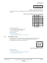
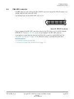
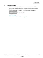
Figure A-5 14-pin F-JTAG ILA connector
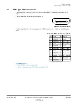
The following table shows the pin mapping for each P
‑
JTAG and SWD signal on the 14
‑
pin F
‑
JTAG ILA
connector.
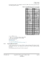
Table A-5 14-pin F-JTAG ILA connector, J17, pin mapping
Pin Signal Pin Signal
1
GND
2
3V3_OUT
3
GND
4
FPGA_TMS
5
GND
6
FPGA_TCK
7
GND
8
FPGA_TDO
9
GND
10
FPGA_TDI
11
NC
12
NC
13
NC
14
NC
Note
• Pins 4, 8, and 10 have pullup resistors to
3V3
.
• Pin 6 has a pulldown resistor to
GND
.
Related information
2.18 System debug
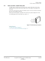
1.3 Location of components on the MPS3 board
A.1.6
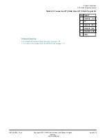
Debug USB 2.0 connector
The MPS3 board provides one USB 2.0 connector that supports configuration file editing in the
microSD, UART access to the FPGA, and CMSIS
‑
DAP FPGA debug using SWD only.
The following figure shows the USB type B connector, J8.
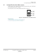
Figure A-6 Debug USB 2.0 connector
Related information
2.18 System debug
1.3 Location of components on the MPS3 board
A Signal descriptions
A.1 Debug connectors
100765_0000_04_en
Copyright © 2017–2020 Arm Limited or its affiliates. All rights
reserved.
Appx-A-75
Non-Confidential


