Programmer’s Model
ARM DDI 0275D
Copyright © 2002, 2003 ARM Limited. All rights reserved.
3-7
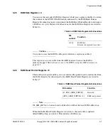
3.2.5
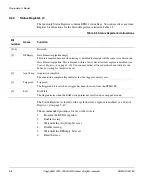
RAM Data Register, r4
You can use the read-only RAM Data Register, while trace capture is disabled, to return
the contents of the ETB11 SRAM location addressed by the RAM Read Pointer
Register. Reading this register increments the RAM Read Pointer Register and triggers
a RAM access cycle. Register bit allocations for the RAM Data Register are listed in
Table 3-6.
Caution
You cannot access the RAM Data Register while trace capture is enabled.
This register is not accessible from the AHB interface because the RAM is
memory-mapped. See
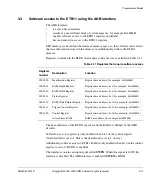
Software access to the ETB11 using the AHB interface
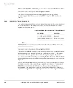
3.2.6
RAM Read Pointer Register, r5
This read/write register enables you to set and read the pointer used to read entries from
the RAM. Register bit allocations for the RAM Read Pointer Register are listed in
Table 3-7.
Note
ETB_ADDR_WIDTH
is a constant used to define the width of the trace RAM address bus.
When the RAM Read Pointer Register is written to, the read address updated
(ReadAddrUp) flag is activated. This initiates a RAM access.
Table 3-6 RAM Data Register bit allocations
Bit
number
Function
[31:0]
RAM data.
Returns the captured trace data.
Table 3-7 RAM Read Pointer Register bit allocations
Bit number
Function
[31: ETB_ADDR_WIDTH]
Reserved
[(ETB_ADDR_WIDTH-1):0]
RAM read pointer
Содержание ETB11
Страница 6: ...List of Tables vi Copyright 2002 2003 ARM Limited All rights reserved ARM DDI 0275D ...
Страница 8: ...List of Figures viii Copyright 2002 2003 ARM Limited All rights reserved ARM DDI 0275D ...
Страница 46: ...Functional Description 2 26 Copyright 2002 2003 ARM Limited All rights reserved ARM DDI 0275D ...
Страница 70: ...Signal Descriptions A 6 Copyright 2002 2003 ARM Limited All rights reserved ARM DDI 0275D ...
Страница 78: ...Glossary Glossary 4 Copyright 2002 2003 ARM Limited All rights reserved ARM DDI 0275D ...

