background image

UG-200 

Evaluation Board User Guide 


Rev. 0 | Page 6 of 28 

EVALUATION BOARD SOFTWARE QUICK START PROCEDURES 

This section provides quick start procedures for using the AD9467, 
either on the evaluation board or at the system level design. 
Both the default and optional settings are described. 

CONFIGURING THE BOARD 

Before using the software for testing, configure the evaluation 
board as follows: 
1.


Connect the evaluation board and the HSC-ADC-EVALCZ 
as shown in Figure 1 and Figure 2. 

2.


Connect one 6 V, 2.5 A switching power supply (such as 
the CUI, Inc., EPS060250UH-PHP-SZ included) to the 
evaluation board.  

3.


Connect one 6 V, 2.5 A switching power supply (such as 
the CUI EPS060250UH-PHP-SZ included) to the HSC-
ADC-EVALCZ board. 

4.


Connect the USB cable to J6 on the HSC-ADC-EVALCZ 
board to the PC. 

5.


On the evaluation board, place jumpers on all four pin 
pairs of P600 to connect the SPI bus. 

6.


On the evaluation board, ensure that P200 is jumpered to 
the off setting to use the on-board 250 MHz Vectron VCC6 
oscillator. 

7.


On the evaluation board, use a clean signal generator with 
low phase noise to provide an input signal to the desired 
channel. Use a 1 m, shielded, RG-58, 50 Ω coaxial cable  
to connect the signal generator. For best results, use a 
narrow-band band-pass filter with 50 Ω terminations  
and an appropriate center frequency. (Analog Devices  
uses TTE, Allen Avionics, and K&L band-pass filters.) 

USING THE SOFTWARE FOR TESTING 

Setting Up the ADC Data Capture 

After configuring the evaluation board, set up the ADC data 
capture block using the following steps: 
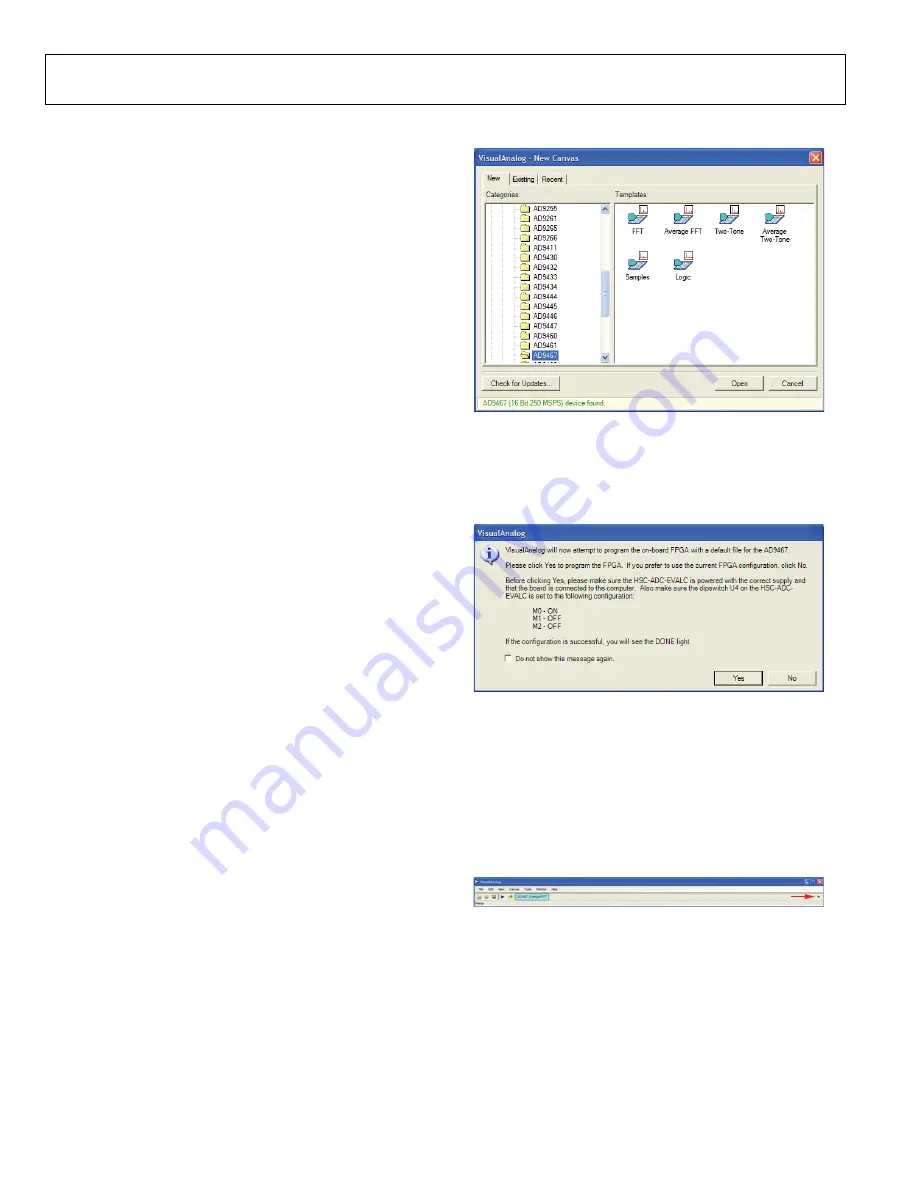
1.


Open VisualAnalog® on a PC. AD9467 should be listed in 
the status bar of the 

New Canvas

 window. Select the 

template that corresponds to the type of testing to be 
performed (see Figure 3). 

09436-

003


Figure 3. VisualAnalog, New Canvas Dialog Box 

2.


After the template is selected, a message box opens, asking 
if the default configuration can be used to program the 
FPGA (see Figure 4). Click 

Yes

, and the window closes. 

If a different program is desired, follow Step 3. 

09436-

004


Figure 4. VisualAnalog, New Canvas Message Box 

3.


To view different channels or change features to settings 
other than the default settings, click the 

Expand Display


button located on the top right corner of the VisualAnalog 
window, as shown in Figure 5 and Figure 6. 
This process is described in the 

AN-905

 Application Note, 

VisualAnalog Converter Evaluation Tool Version 1.0 User 
Manual

. Once you are finished, click the 

Collapse Display


button. 

09436-

005

EXPAND DISPLAY BUTTON


Figure 5. VisualAnalog Window Toolbar, Expand Display Button 

Содержание UG-200

Страница 1: ...7 data sheet HSC ADC EVALCZ data sheet High Speed Converter Evaluation Platform FPGA based data capture kit AN 905 ApplicationNote VisualAnalog Converter Evaluation Tool Version 1 0 User Manual AN 878...

Страница 2: ...vision History 2 Evaluation Board Hardware 3 Power Supplies 3 Input Signals 3 Output Signals 3 Default Operation and Jumper Selection Settings 5 Evaluation Board Software Quick Start Procedures 6 Conf...

Страница 3: ...bles the user to bias each section of the board individually Use P700 and P701 to connect a different supply for each section At least one 1 8 V supply is needed with a 1 A current capability for 1 8...

Страница 4: ...8 09436 002 SIGNAL SYNTHESIZER CLOCK INPUT WALL OUTLET 100V TO 240V AC 47Hz TO 63Hz SWITCHING POWER SUPPLY SWITCHING POWER SUPPLY PC RUNNING ADC ANALYZER OR VisualAnalog USER SOFTWARE ANALOG INPUT SIG...

Страница 5: ...led circuit using a high bandwidth 1 1 impedance ratio transformer T201 that adds a very low amount of jitter to the clock path The clock input is 50 terminated and ac coupled to handle single ended s...

Страница 6: ...ble to connect the signal generator For best results use a narrow band band pass filter with 50 terminations and an appropriate center frequency Analog Devices uses TTE Allen Avionics and K L band pas...

Страница 7: ...oller After the ADC data capture board setup has been completed set up the SPI Controller 1 Open the SPI Controller software by going to the Start menu or double clicking the SPI Controller software d...

Страница 8: ...r Very Low Signal Applied 09436 012 Figure 12 VisualAnalog FFT Graph Full Scale Signal Applied 09436 013 Figure 13 Typical FFT AD9467 No Buffer Current Optimization 2 To optimize SFDR performance use...

Страница 9: ...tion Board User Guide UG 200 Rev 0 Page 9 of 28 09436 015 Figure 15 SPI Controller SPI Controller BUFFER 36 BUFFER 107 Drop Down Setting 09436 016 Figure 16 Typical FFT AD9467 With Buffer Current Opti...

Страница 10: ...N P C112 711C 811C R120 R119 R112 R111 6 4 2 3 1 T101 5 4 3 1 T102 5 4 3 1 T100 ADL5562_PRELIM DNI 0 1UF 0 1UF DNI 0 1UF 0 1UF DNI 0 1UF 0 1UF DNI DNI 0 1UF 0 1UF 0 1UF 0 1UF 0 1UF 0 1UF 0 1UF 0 1UF...

Страница 11: ...2 1 J200 C204 C207 C203 C202 1 2 3 CR200 C210 C209 6 4 2 3 1 T201 5 4 3 1 T200 DNI 0 1UF 0 1UF 0 1UF DNI 0 1UF 0 1UF 0 1UF 0 1UF DNI DNI OPT_CLK_P AVDD_3P3V OPT_CLK_N MABA 007159 000000 200 DNI CLK CL...

Страница 12: ...0 1UF 0 1UF DNI 0 1UF 0 1UF DNI 0 1UF DNI 0 1UF OPT_CLK_N 0 1UF 0 1UF DNI DNI OPT_CLK_P DNI 0 1UF 0 1UF 0 1UF 0 1UF 0 1UF 0 1UF 0 1UF 0 1UF 0 1UF LNJ314G8TR A GREEN 1 00K AD9517_CSB 0 249 DNI 22UF 4...

Страница 13: ...6 5 45 43 41 14 46 44 42 13 37 18 38 17 27 28 30 29 26 25 24 23 22 21 36 35 34 33 32 31 20 19 50 16 10 69 68 65 64 12 11 9 8 7 4 3 72 71 70 63 62 2 61 60 59 58 56 55 54 53 52 15 1 DUT1 1 TP401 C436 A...

Страница 14: ...D6 D5 D4 D3 D2 D10 D1 P501 B9 B8 B7 B6 B5 B4 B3 B2 B10 B1 P501 A9 A8 A7 A6 A5 A4 A3 A2 A10 A1 P501 DG9 DG8 DG7 DG6 DG5 DG4 DG3 DG2 DG10 DG1 P502 BG9 BG8 BG7 BG6 BG5 BG4 BG3 BG2 BG10 BG1 P502 C9 C8 C7...

Страница 15: ...DD1_DUT AVDD1_DUT NC7WZ07P6X TSW 104 08 G D 10K 1 00K 0 1UF 1 00K 0 1UF 10K 10K NC7WZ16P6X 1 00K AVDD_3P3V AVDD_3P3V SCLK CSB CSB_USB SCLK_USB SDI_USB SDO_USB SDIO Y2 Y1 A2 A1 GND VCC VCC Y1 A1 A2 GND...

Страница 16: ...3 R7 ADP1708ARDZ R7 ADP1708ARDZ R7 0 01UF 0 01UF 0 1UF 0 1UF 0 1UF 0 1UF 750 45OHMS 4 7UF 1K 4 7UF 348 1K PWR_IN2 Z5 531 3425 0 3P3V_AVDD Z5 531 3425 0 DUT_AVDD2 DUT_DRVDD 45OHMS 45OHMS DRVDD_DUT 10UF...

Страница 17: ...Evaluation Board User Guide UG 200 Rev 0 Page 17 of 28 09436 024 Figure 24 Top Layer 1...

Страница 18: ...UG 200 Evaluation Board User Guide Rev 0 Page 18 of 28 09436 025 Figure 25 Ground Layer 2...

Страница 19: ...Evaluation Board User Guide UG 200 Rev 0 Page 19 of 28 09436 026 Figure 26 Power Plane Layer 3...

Страница 20: ...UG 200 Evaluation Board User Guide Rev 0 Page 20 of 28 09436 027 Figure 27 Ground Plane Layer 4...

Страница 21: ...Evaluation Board User Guide UG 200 Rev 0 Page 21 of 28 09436 028 Figure 28 Ground Plane Layer 5...

Страница 22: ...UG 200 Evaluation Board User Guide Rev 0 Page 22 of 28 09436 029 Figure 29 Power Plane Layer 6...

Страница 23: ...Evaluation Board User Guide UG 200 Rev 0 Page 23 of 28 09436 030 Figure 30 Ground Plane Layer 7...

Страница 24: ...UG 200 Evaluation Board User Guide Rev 0 Page 24 of 28 09436 031 Figure 31 Bottom Side Layer 8...

Страница 25: ...F 6 3 V X5R 0201 Murata GRM033R60J104KE19D 8 8 C708 C709 C710 C715 C716 C717 C718 C720 Capacitor ceramic 4 7 F 6 3 V X5R 0603 Murata GRM188R60J475KE19D 9 2 C713 C719 Capacitor 10 000 pF 0402 16 V cera...

Страница 26: ...sonic ERJ 2GEJ512X 36 1 R316 Resistor 200 1 10 W 1 0402 SMD Panasonic ERJ 2RKF2000X 37 2 R103 R130 Resistor 20 1 20 W 5 0201 SMD Panasonic ERJ 1GEJ200C 38 2 R311 R313 Resistor 100 1 10 W 5 0402 SMD Pa...

Страница 27: ...of assembly 100 mil jumpers place into P100 Pin 2 to Pin 3 P200 Pin 1 to Pin 2 J300 Pin 3 to Pin 4 P600 Pin 1 to Pin 2 Pin 3 to Pin 4 Pin 5 to Pin 6 Pin 7 to Pin 8 SAMTEC SNT 100 BK G H 53 4 MP111 MP1...

Страница 28: ...party for any reason Upon discontinuation of use of the Evaluation Board or termination of this Agreement Customer agrees to promptly return the Evaluation Board to ADI ADDITIONAL RESTRICTIONS Custom...

Отзывы: