background image

UG-478 

Evaluation Board User Guide 


Rev. 0 | Page 16 of 40 

SOFTWARE OPERATION 

Overview of the Main Window 

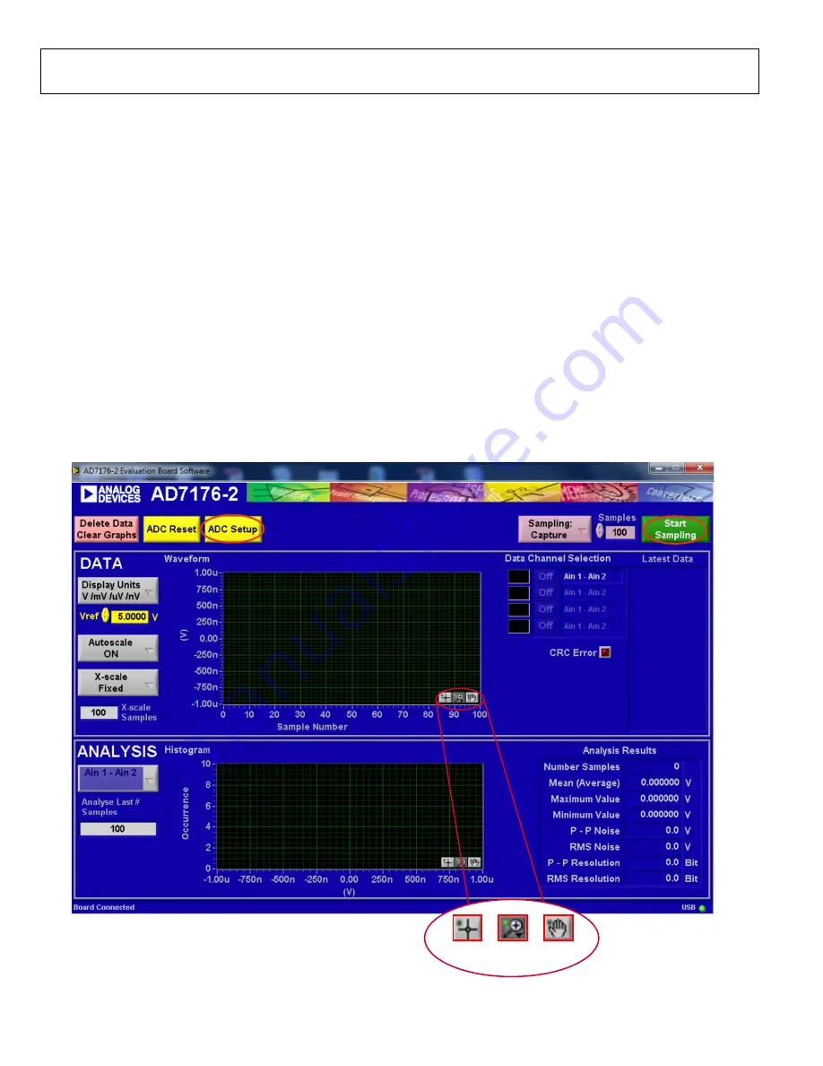
The main window of the software (see Figure 20) contains the 
significant control buttons and analysis indicators of the 

AD7176-2

 software. 

ADC Setup Button 

Clicking 

ADC Setup

, located near the top left of the main 

window (see Figure 20), opens the 

AD7176-2 Register Interface


window. 

Start Sampling Button 

Clicking 

Start Sampling

, located near the top right hand corner 

of the main window (see Figure 20), starts ADC sampling; results 
are reported in the graphs of the 

DATA

 and 

ANALYSIS

 sections 

of the main window. 

Data Graph 

The graph in the upper half, or 

DATA

 section, of the main window, 

shows each successive sample of the ADC output (input referred).  

The indicators beside this graph show the latest data value, the 
channel being converted, and the flag for the error diagnostics 
of the 

AD7176-2

. Navigation tools are provided to allow you to 

control the cursor, zooming, and panning (see Figure 20). 

Analysis Graph 

The graph in the bottom half, or 

ANALYSIS

 section, of the 

main window, shows the histogram analysis; to the right of the 
graph, the respective noise analysis on the indicator is shown. 
Navigation tools are provided to allow you to control the cursor, 
zooming, and panning (see Figure 20). 

CRC Error Indicator 

This LED icon illuminates when there has been a CRC error 
detected in the communications between the software and the 

AD7176-2

. The CRC functionality on the 

AD7176-2

 is disabled 

by default. 

Exiting the Software 

To exit the software, click the red X at the top right hand corner 
of the main window.  


Figure 20. Main Window 


1

1035-

017

NOTES
1. FOR DETAILS ABOUT THE AREAS HIGHLIGHTED IN RED, SEE THE OVERVIEW

OF THE MAIN WINDOW SECTION.

CONTROL

CURSOR

CONTROL

ZOOMING

CONTROL

PANNING

Содержание EVAL-AD7176-2SZD

Страница 1: ... V external bench top supply is regulated to 5 V and 3 3 V to supply the AD7176 2 and support all necessary components The EVAL AD7176 2SDZ board connects to the USB port of the PC by connection to the EVAL SDP CB1Z motherboard The EVAL AD7176 2SDZ software fully configures the AD7176 2 device register functionality and provides dc time domain analysis in the form of waveform graphs histograms and...

Страница 2: ...e Description 4 Hardware Link Options 4 Power Supplies 6 Serial Interface 6 Analog Inputs 6 Sockets Connectors 7 Reference Options 8 Using the On Board Amplifiers 8 Evaluation Board Setup Procedures 11 Evaluation Board Software 12 Software Installation Procedures 12 Setting Up the System for Data Capture 15 Software Operation 16 Evaluation Board Schematics and Artwork 21 EVAL AD7176 2SDZ Bill of M...

Страница 3: ...ds together using the plastic screw washer set included in the evaluation board kit to ensure that the boards are connected firmly together 3 Apply an external voltage in the range of 7 V to 9 V to the J4 or J5 connecter of the EVAL AD7176 2SDZ board as shown in Figure 2 see Table 3 for more information This provides the power supply for the board 4 Connect the EVAL SDP CB1Z board to the PC using ...

Страница 4: ... 3 3 V when AVDD1 equals 2 5 V and AVSS equals 2 5 V SL2 A Sets the voltage applied to the AVDD1 pin In Position A this link sets the voltage applied to the AVDD1 pin to be a 5V supply from the ADP1720 5 U7 regulator or a 2 5 V supply from the ADP1720 U4 regulator In Position B this link sets the voltage applied to the AVDD1 pin to be supplied from an external voltage source via Connector J9 When ...

Страница 5: ...before being applied to the AIN0 pin With this link in Position C the analog input path includes the ADA4940 1 differential amplifier therefore in conjunction with AIN1 a single ended to differential driver is implemented With this link in Position D AIN0 is connected to Header J10 AVSS to AGND When these links are inserted AVSS is tied to AGND When AVSS is set to 2 5 V these links must be removed...

Страница 6: ...Z in standalone mode the AD7176 2 serial interface lines can be disconnected from the 120 pin header by removing the 0 Ω links R9 through R13 The test points can then be used to fly wire the signals to an alternative digital capture setup ANALOG INPUTS The EVAL AD7176 2SDZ primary analog inputs can be applied in two ways Using J8 the green screw in terminal connector on the right hand side of the ...

Страница 7: ...C 1 5 3 G 3 81 Farnell 3704737 J5 External wall wart voltage supply 7V to 9V for EVAL AD7176 2SDZ DC power connectors 2 mm SMT power Jack Kycon KLDX SMT2 0202 A Mouser 806 KLDX SMT20202A J8 Analog input screw terminal block wired connection to external source or sensor 8 pin terminal header 3 81 mm pitch vertical Phoenix Contact MC 1 5 8 G 3 81 Farnell 3704774 J9 External benchtop voltage supply o...

Страница 8: ... that enables the internal reference Figure 3 Selecting the Reference Source for Setup 1 Setup 2 Setup 3 and Setup 4 Figure 4 Turning On the Internal 2 5 V Reference USING THE ON BOARD AMPLIFIERS The AD7176 2 evaluation board contains three front end configu rations The AD8656 is provided for buffering the analog inputs of the AD7176 2 By default it is configured for a gain of 2 and the front end ...

Страница 9: ...59 270 pF C28 270 pF C23 680 pF C26 680 pF 1 Remove R72 and R100 when connecting the ADA4940 1 to the AD7176 2 2 Remove R110 and R120 when connecting the AD8475 to the AD7176 2 0 1µF 5V R91 R92 R105 R72 R100 R34 R39 R65 R93 AD8656 R68 R106 R99 IN0 IN1 C19 C59 C23 0 1µF R119 5V R126 R115 R110 R47 R125 R120 R46 R107 R117 AD8656 R116 R109 IN2 IN3 C28 C27 C26 3 REF 2 REF 21 AIN0 22 AIN1 23 AIN2 4 REFO...

Страница 10: ...ponents for AD8475 Attenuating Single Ended to Differential Driver Component Status R63 0 Ω R641 Not inserted R741 Not inserted R78 0 Ω R46 0 Ω R47 0 Ω C27 270 pF C28 270 pF C26 680 pF 1 Populate R64 and R74 with 10 Ω resistors to connect the AD8475 to the AD7176 2 and place the SL9 and SL10 solder links in Position C Ensure that the R110 and R120 resistors are removed 11035 036 R96 R97 R34 R39 C1...

Страница 11: ...iguring the Evaluation and SDP Boards 1 Connect the EVAL SDP CB1Z board to Connector A or Connector B on the EVAL AD7176 2SDZ board Screw the two boards together using the plastic screw washer set included in the evaluation board kit to ensure that the boards are connected firmly together 2 Connect the power supplies to the EVAL AD7176 2SDZ board The EVAL AD7176 2SDZ board requires an external ben...

Страница 12: ...e USB port of the PC insert the installation CD into the CD ROM drive 2 Double click the setup exe file to begin the evaluation board software installation The software is installed to the following default location C Program Files Analog Devices AD7176 2 3 A dialog box appears asking for permission to allow the program to make changes to your computer Click Yes Figure 8 AD7176 2 Evaluation Softwa...

Страница 13: ...lick Next to continue Figure 11 AD7176 2 Evaluation Software Installation Reviewing a Summary of the Installation 7 A dialog box informs you when the installation is complete Click Next Figure 12 AD7176 2 Evaluation Software Installation Indicating When the Installation Is Complete 11035 008 11035 009 ...

Страница 14: ...ers Setup Beginning the Drivers Installation 2 Select the location to install the drivers and then click Next Figure 14 EVAL SDP CB1Z Drivers Setup Selecting the Location for Drivers Installation 3 Click Install to confirm that you would like to install the drivers Figure 15 EVAL SDP CB1Z Drivers Setup Granting Permission to Install Drivers 4 To complete the drivers installation click Finish which...

Страница 15: ...Tools see Figure 18 b The EVAL SDP CB1Z board should appear under ADI Development Tools This indicates that the driver software is installed and that the board is connecting to the PC correctly Figure 18 Device Manager Checking That the Board Is Connected to the PC Correctly Launching the Software After completing the steps in the Setting Up the System for Data Capture section launch the AD7176 2 ...

Страница 16: ...latest data value the channel being converted and the flag for the error diagnostics of the AD7176 2 Navigation tools are provided to allow you to control the cursor zooming and panning see Figure 20 Analysis Graph The graph in the bottom half or ANALYSIS section of the main window shows the histogram analysis to the right of the graph the respective noise analysis on the indicator is shown Naviga...

Страница 17: ... to AIN3 conversion is mapped using the Setup 1 configuration c Setup 1 is configured with the following register settings i In the SETUPCON1 register the external reference is selected as the reference source for the ADC conversion ii In the FILTCON1 register the output data rate is set to 1 kHz and the fast settling filter Sinc5 Sinc1 is enabled iii In the OFFSET1 register the default offset reg...

Страница 18: ...sed on the value set in this box 2 Select the number of samples to analyze in the Samples box Note that when performing a continuous capture this number is limited to 65 536 samples 3 When Sampling is set to Capture a batch of samples is read when Start Sampling is clicked with the batch size being set by the value in the Samples box When Sampling is set to Continuous the software performs a conti...

Страница 19: ...el is selected and the value of the last sample of the batch The conversions can be displayed as codes or as volts DC Testing Histogram The histogram resulting from the gathered samples is shown in the bottom graph Parameters such as peak to peak noise and rms noise are displayed to the right of the graph in the Analysis Results section for the current batch of samples Figure 23 Waveform and Histo...

Страница 20: ...captured data for later analysis see Figure 24 1 Right click on the waveform or histogram graph 2 Select Export Data from the drop down menu that appears A Save dialog box is displayed prompting you to save the data to an appropriate folder location Figure 24 Exporting Data to Save Results 11035 019 ...

Страница 21: ...Evaluation Board User Guide UG 478 Rev 0 Page 21 of 40 EVALUATION BOARD SCHEMATICS AND ARTWORK Figure 25 Schematic AD7176 2 11035 022 ...

Страница 22: ...UG 478 Evaluation Board User Guide Rev 0 Page 22 of 40 Figure 26 Schematic Amplifiers 11035 033 ...

Страница 23: ...Evaluation Board User Guide UG 478 Rev 0 Page 23 of 40 Figure 27 Schematic Power Supply Sequencing 11035 023 ...

Страница 24: ...UG 478 Evaluation Board User Guide Rev 0 Page 24 of 40 Figure 28 Schematic Regulators 11035 024 ...

Страница 25: ...Evaluation Board User Guide UG 478 Rev 0 Page 25 of 40 Figure 29 Schematic SDP Connector 11035 025 ...

Страница 26: ...8 99 100 101 102 103 104 105 106 107 108 109 110 111 112 113 114 115 116 117 118 119 120 121 122 1 2 3 4 1 2 3 4 5 6 7 8 1 2 1 2 1 2 3 4 5 1 2 3 4 5 6 7 8 9 10 1 2 1 2 1 2 1 2 1 2 1 2 3 1 2 3 4 5 6 1 2 3 1 2 1 2 B E C 1 2 1 2 1 2 1 2 1 2 1 2 1 2 1 2 1 2 1 2 1 2 1 2 1 2 1 2 1 2 1 2 3 1 2 3 4 5 1 2 3 4 5 1 2 3 4 5 1 2 3 4 5 1 2 3 4 5 1 2 3 4 5 1 2 3 4 5 1 2 3 4 1 1 1 1 1 1 1 1 1 1 1 1 1 1 1 1 1 1 1 ...

Страница 27: ...Evaluation Board User Guide UG 478 Rev 0 Page 27 of 40 Figure 32 Bottom Printed Circuit Board PCB Silkscreen Figure 33 Layer 1 Component Side 11035 028 11035 029 ...

Страница 28: ...UG 478 Evaluation Board User Guide Rev 0 Page 28 of 40 Figure 34 Layer 2 Ground Plane Figure 35 Layer 3 Power Ground Plane 11035 030 11035 031 ...

Страница 29: ...Evaluation Board User Guide UG 478 Rev 0 Page 29 of 40 Figure 36 Layer 4 Component Side 11035 032 ...

Страница 30: ...POINT SMALL Test point not inserted keep hole clear of solder N A N A Do not insert AIN4 TESTPOINT SMALL Test point not inserted keep hole clear of solder N A N A Do not insert C1 4 7 µF 10 C0603 Ceramic capacitor 6 3 V X5R 0603 Murata GRM188R60J47 5K FEC 173 5527 C2 0 1 µF 10 C0603 Ceramic capacitor 50 V X7R 0603 Murata GRM188R71H1 04K FEC 882 0023 C3 4 7 µF 10 C0603 Ceramic capacitor 10 V X5R 06...

Страница 31: ...eramic capacitor 25V NPO 0402 AVX 04023A271JAT 2A FEC 132 7623 C30 4 7 µF 10 C0603 Ceramic capacitor 6 3 V X5R 0603 Murata GRM188R60J47 5K FEC 173 5527 C31 0 1 µF 10 C0402 Ceramic capacitor 16 V X7R 0402 Murata GRM155R71C1 04K FEC 881 9742 C32 10 µF 10 1210 Ceramic capacitor 50 V X5R 1210 Murata GRM32ER61H1 06K FEC 184 5764 C33 0 1 µF 10 C0402 Ceramic capacitor 16 V X7R 0402 Murata GRM155R71C1 04K...

Страница 32: ...itor 16 V X7R 0402 Murata GRM155R71C1 04K FEC 881 9742 C59 270 pF 5 R0402 Ceramic capacitor 25V NPO 0402 AVX 04023A271JAT 2A FEC 132 7623 C60 0 1 µF 10 C0402 Ceramic capacitor 16 V X7R 0402 Murata GRM155R71C1 04K FEC 881 9742 C61 C0603 Ceramic capacitor not inserted 0603 N A N A Do not insert C62 C0603 Ceramic capacitor not inserted 0603 N A N A Do not insert C63 C0603 Ceramic capacitor not insert...

Страница 33: ...ot inserted keep hole clear of solder N A N A Do not insert GND2 TESTPOINT SMALL Test point not inserted keep hole clear of solder N A N A Do not insert GND3 TESTPOINT SMALL Test point not inserted keep hole clear of solder N A N A Do not insert GND4 TESTPOINT SMALL Test point not inserted keep hole clear of solder N A N A Do not insert GND5 TESTPOINT SMALL Test point not inserted keep hole clear ...

Страница 34: ...unt Harwin M20 9990246 FEC 1022247 and 150 411 LK9 SIP 2P 2 pin 0 1 pitch header and shorting shunt Harwin M20 9990246 FEC 1022247 and 150 411 Q1 SOT23 MOSFET transistor Vishay Siliconix SI2304DDS T1 GE3 FEC 1858939 Q2 SOT23 Transistor NPN SOT 23 ON Semiconductor MMBT3904LT1G FEC 1459100 R1 DNI 0 01 R0603 Resistor not inserted 0603 N A N A Do not insert R2 100k 0 01 R0603 SMD resistor Multicomp MC...

Страница 35: ...402 Vishay CRCW0402000 0Z0ED FEC 146 9661 R31 DNI 0 01 R0402 Resistor not inserted 0402 N A N A Do not insert R32 0R 0 01 R0402 Resistor 0402 Vishay CRCW0402000 0Z0ED FEC 146 9661 R33 DNI 0 01 R0402 Resistor not inserted 0402 Vishay CRCW0402000 0Z0ED Do not insert R34 0R 0 01 R0402 Resistor 0402 Vishay CRCW0402000 0Z0ED FEC 146 9661 R35 0R 0 01 R0402 Resistor 0402 Vishay CRCW0402000 0Z0ED FEC 146 ...

Страница 36: ...A FEC 146 9739 R66 1k 0 01 R0603 Resistor 0603 thick film 1 Vishay Draloric CRCW06031K0 0FKEA FEC 1469740 R67 DNI 0 01 R0603 Resistor not inserted 0603 Vishay Draloric CRCW0603000 0Z0EA Do not insert R68 1k 0 1 R0603 Resistor 0603 Panasonic ERA3AEB102V FEC 157 7605 R69 DNI 0 01 R0603 Resistor not inserted 0603 N A N A Do not insert R70 0R 0 01 R0402 Resistor 0402 Vishay CRCW0402000 0Z0ED FEC 146 9...

Страница 37: ...not insert R97 DNI 0 01 R0603 Resistor not inserted 0603 Vishay Draloric CRCW0603000 0Z0EA Do not insert R98 0R 0 01 R0603 Resistor 0603 Vishay Draloric CRCW0603000 0Z0EA FEC 146 9739 R99 1k 0 1 R0603 Resistor 0603 Panasonic ERA3AEB102V FEC 157 7605 R100 0R 0 01 R0603 Resistor 0603 Vishay Draloric CRCW0603000 0Z0EA FEC 146 9739 R101 0R 0 01 R0603 Resistor 0603 Vishay Draloric CRCW0603000 0Z0EA FEC...

Страница 38: ... insert SL1 0603 2WAY BRIDGE 2 way solder link use 0 Ω 0603 resistor insert in Link Position A N A FEC 933 1662 SL2 0603 2WAY BRIDGE 2 way solder link use 0 Ω 0603 resistor insert in Link Position A N A FEC 933 1662 SL3 0603 2WAY BRIDGE 2 way solder link use 0 Ω 0603 resistor insert in Link Position A N A FEC 933 1662 SL4 0603 3WAY BRIDGE 3 way solder link use 0 Ω 0603 resistor insert in Link Posi...

Страница 39: ...Devices ADP7104ARDZ 5 0 ADP7104ARDZ 5 0 U3 MSO10 Quad voltage monitor and sequencer Analog Devices ADM1185ARMZ 1 ADM1185ARMZ 1 U4 MSO8 50 mA high voltage micropower linear regulator adjustable Analog Devices ADP1720ARMZ R7 ADP1720ARMZ R7 U5 TSSOP24 2 4 channel 250 kSPS 24 bit multiplexed Σ Δ ADC Analog Devices AD7176 2BRUZ AD7176 2BRUZ U6 SO8NB 5 V XFET reference Analog Devices ADR445BRZ ADR445BRZ...

Страница 40: ...y other party for any reason Upon discontinuation of use of the Evaluation Board or termination of this Agreement Customer agrees to promptly return the Evaluation Board to ADI ADDITIONAL RESTRICTIONS Customer may not disassemble decompile or reverse engineer chips on the Evaluation Board Customer shall inform ADI of any occurred damages or any modifications or alterations it makes to the Evaluati...

Отзывы: