AD9956/PCB
Rev. 0 | Page 5 of 12
CONTROL DIALOG BOX
Use the
Control
dialog box to enable and disable individual
device functions, program the input clock speed, and toggle
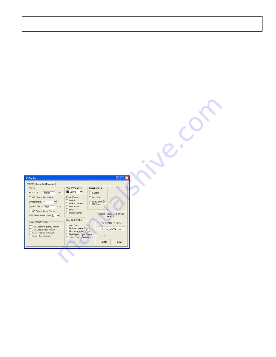
various other options. Figure 3 shows the sections of the
Control
dialog box:
Clock
,
Output Waveform
,
Linear Sweep
,
Power Down
,
Accumulator Control
, and
Sync Multi DUT’s
.
Click
Charge Pump/Clock Driver Window
,
I/O Interface
Window,
or
DUT Signals Window
to access these dialog
boxes.
LOAD and READ
At the bottom right of the dialog box are the
LOAD
and
READ
buttons.
After you have made changes to the evaluation software, click
LOAD
to send the data to the device. In addition to sending
data, you can also configure
LOAD
to automatically send an
I/O update signal to the DUT when the software finishes
sending data. See the DUT Signals Dialog Box section for
details. When new data is ready to be sent,
LOAD
flashes
green, indicating that a you need to issue a
LOAD
.
Click
READ
to perform a readback of the currently program-
med status of the device and to update the GUI with the current
settings.
05278-
003
Figure 3. Control Dialog Box
Clock
To program the reference clock and the RF prescalar values:
1.
In the
Ref Clock
box, type the operating frequency of the
external reference clock. The maximum is 2.7 GHz.
2.
In the
Divider Ratio
box, select a divider value for the RF
prescalar. The value must be in the range of 1 and 8.
3.
Click
LOAD
.
To bypass the RF divider and pipe the REFCLK input directly to
the DDS core, select
RF Divider RefClk Mux
. Even though the
divider operates at /1, /2, /4, or /8, and this divided signal can be
ported to the PECL driver, the raw, undivided REFCLK is used
as the internal system clock when this box is checked. Do
not
select this box, if the REFCLK input is greater than 400 MHz.
Output Waveform
In the
Output Waveform
box, select either a cosine(x) or a
sine(x) function for the angle-to-amplitude conversion.
Linear Sweep
Use the
Linear Sweep
section to enable the linear sweep
functions of the DDS. See the AD9956 data sheet for a detailed
explanation of these modes of operation.
Select
Enable
to turn on the frequency accumulator. If the
No
Dwell
box is not checked, the part is set in ordinary linear
sweep mode.
Select both
Enable
and
No Dwell
to put the part into linear
sweep no-dwell mode.
When you select
Load SRR @ I/O Updat
e, the current
countdown of the sweep ramp rate is cleared every time an
I/O_UPDATE signal is sent to the part. When using manual
programming through the GUI, it is almost impossible to notice
the effect of this function because the sweep ramp rates cycle
through their countdown timers in less than 655 µs, even when
programmed to a maximum value.
The linear sweep parameters (delta frequencies and ramp rates)
are controlled in the
Linear Sweep
section (see Figure 3). The
sweep itself, however, is controlled by the
Ramp Up
and
Ramp
Down
buttons, which appear at the bottom of the
Profile
dialog
box when the
Linear Sweep Enable
box is checked. See the
Profile Dialog Box section for details.
Power Down
In the
Power Down
section, select the check boxes for the
circuit blocks that you want to power down.
Accumulator Control
This section controls the clear functions for the phase and
frequency accumulators.
Select
Auto Clear Frequency Accum.
or
Auto Clear Phase
Accum.
to clear and release the corresponding accumulator.
The auto clear function sets the accumulator to a known value
of 0 and then begins accumulating.
Содержание AD9953YSVZ
Страница 11: ...AD9956 PCB Rev 0 Page 11 of 12 NOTES...


