background image

AD9956/PCB 


Rev. 0 | Page 8 of 12 

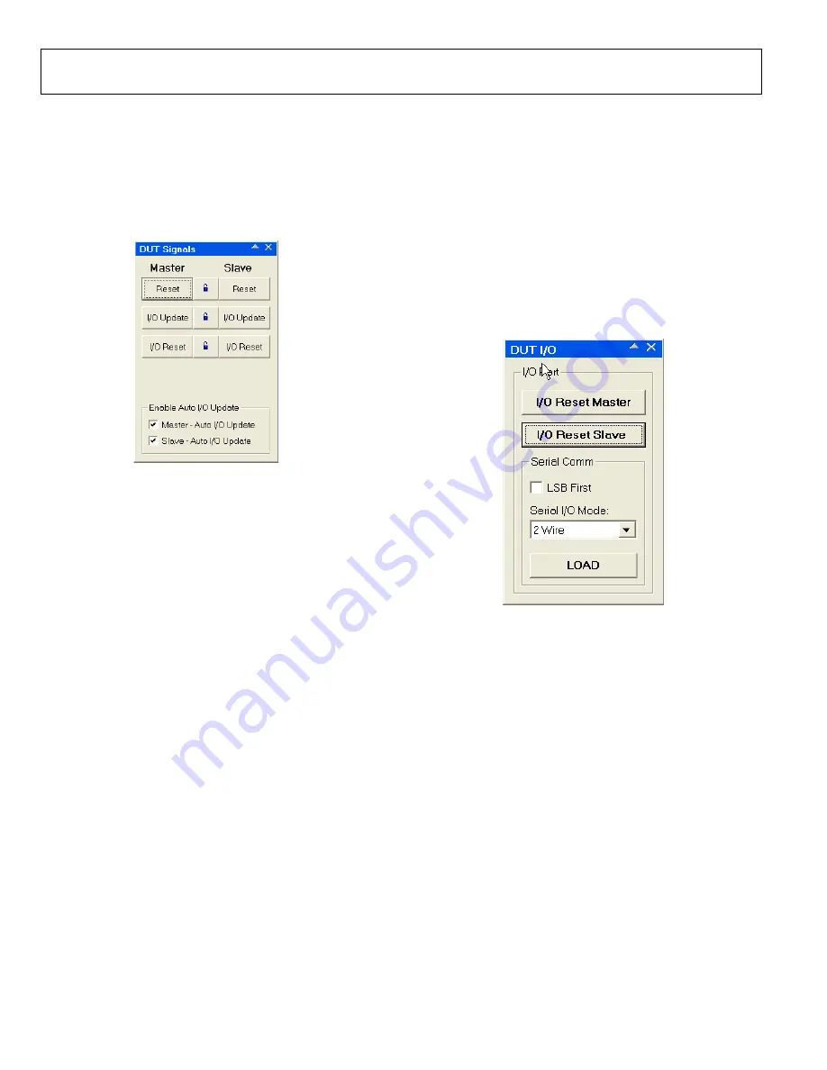
DUT SIGNALS DIALOG BOX 

This dialog box controls the reset, I/O update, and I/O reset 
signals for the master and slave devices. Click the lock icon 
between the corresponding Master and Slave buttons to lock the 
two together. Click 

Master

 or 

Slave


Reset

I/O Update

, or 

I/O 

Reset

,  to specify the unit that issues the command to both 

devices.  

05278-007


Figure 7. DUT Signals Dialog Box 

The auto I/O update function is controlled in the 

Enable Auto 

I/O Update 

section. Select either 

Master–Auto I/O Update,


Slave–Auto I/O Update

, or both to send an I/O update to the 

device(s) every time you click 

LOAD

 (default on). If you want a 

device to wait for a manually sent I/O update signal, clear the 
corresponding check box. 

DUT I/O DIALOG BOX 

This dialog box controls the I/O configuration for the device.  

Click 

I/O Reset Master

 or 

I/O Reset Slave

 to send an I/O reset 

to the corresponding serial port state machine. 

Select 

LSB First

 to change the data format to LSB first. The 

default is MSB first. 

In the 

Serial I/O Mode

 section, select either 

2 Wire

 or 

3 Wire


from the drop-down list to specify the part as either, respectively, 
a 2-wire serial port, in which the serial data line is I/O, or a 
3-wire serial port, in which the serial data is input on SDI/O 
and read back on SDO. 


05278-008


Figure 8. DUT I/O Dialog Box 

Содержание AD9953YSVZ

Страница 1: ...781 326 8703 2005 Analog Devices Inc All rights reserved EVALUATION BOARD FUNCTIONAL BLOCK DIAGRAM M DDS R VCO N LPF AD9956 LPF VCO AND LOOP FILTER ONLY POPULATED ON AD9956 VCO PCB THESE SOCKETS LEFT...

Страница 2: ...nning and Using the Software 4 Control Dialog Box 5 Profile Dialog Box 6 Clock Driver Control Phase Frequency Detector Charge Pump Dialog Box 7 DUT Signals Dialog Box 8 DUT I O Dialog Box 8 Debug Wind...

Страница 3: ...ind of application the external signal should be applied to the DUT REF IN connector J2 This leads to the AD9956 Pins PLLREF PLLREF the reference input of the AD9956 s phase frequency detector See the...

Страница 4: ...Program Files ADI AD9956 Evaluation Software 2 Double click the icon to launch the evaluation software A status window similar to Figure 2 appears in the center of the AD9956 Evaluation Software dial...

Страница 5: ...raw undivided REFCLK is used as the internal system clock when this box is checked Do not select this box if the REFCLK input is greater than 400 MHz Output Waveform In the Output Waveform box select...

Страница 6: ...output The PLL lock detect enable bit in the Charge Pump dialog box enables a PLL lock monitoring function either through the PLL_LOCK_DETECT pin externally or by setting a flag in the control regist...

Страница 7: ...ntire charge pump A delay occurs when coming out of this power down to reestablish the correct charge pump current Select Charge Pump Quick Powerdown to power down the phase detector logic while keepi...

Страница 8: ...end an I O update to the device s every time you click LOAD default on If you want a device to wait for a manually sent I O update signal clear the corresponding check box DUT I O DIALOG BOX This dial...

Страница 9: ...The Debug Window shown in Figure 9 lets you directly write to any of the internal registers and subsequently read them back You can also directly toggle the states of any external inputs such as PS0...

Страница 10: ...harge sensitive device Electrostatic charges as high as 4000 V readily accumulate on the human body and test equipment and can discharge without detection Although this product features proprietary ES...

Страница 11: ...AD9956 PCB Rev 0 Page 11 of 12 NOTES...

Страница 12: ...AD9956 PCB Rev 0 Page 12 of 12 NOTES 2005 Analog Devices Inc All rights reserved Trademarks and registered trademarks are the property of their respective owners EB05278 0 1 05 0...

Отзывы: