background image

Evaluation Board User Guide 

UG-207


Rev. A | Page 15 of 16 

The 

RAM I/O Window 

allows you to easily interface RAM data 

into the AD9910. Use the 

RAM Data File

 box to locate the 

RAM file on the PC. Use the 

Data Format 

drop-down box to 

select the file format. The options are: 

RAW Binary

RAW Hex

and 

RAW Decimal.

 Use the 

Load File 

button to transfer the 

data to the AD9910. The 

Read RAM to File 

button allows you 

to read the data from the RAM to a file in the same folder as the 
evaluation board software. The 

Output Data Format 

allows 

you to select the format of the output file. The options are: 

RAW Binary

RAW Hex

, and 

RAW Decimal. 

Use the 

Open 

File in Notepad 

check box to view the file immediately.  
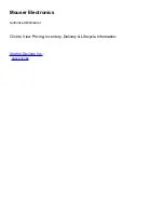
DEBUG 

To access the 

Debug

 window, select 

Debug Window

 from the 

View 

drop-down menu (see Figure 10). 

07

48

1-

0

13


Figure 15. Debug Window 

The 

Debug 

window gives you complete direct access to the 

register map as well as control of many external pins. The 

Debug


window is intended for debugging issues with the AD9910. It 
can be used for all programming, but is not user-friendly; this 
may result in improper programming of reserved bits. 

DUT Signals (PA) 

The 

ISFC

ExtPwrDwn

Reset DUT

I/O Reset

, and 

CSB

 check 

boxes control the pins to which they correspond. All of these 
functions are available elsewhere in the software. A check in the 
box means that the pin is in its active state. Note that this does 
not mean that the pin is logic high or low. This is determined by 
the active state on that pin. See the AD9910 data sheet for 
information about external pins. The 

Flash 

and 

USB_Status


check boxes are used to control the two LEDs on the AD9910 
evaluation board.  

DUT Signals (PE) 

The 

REGUD_EN

DRCTL

DRHOLD

REGUD

OSK

P3

P2

and 

P1

 check boxes control their selected pins. 

REGUD

 issues an 

I/O update to the device under test (DUT), whereas 

REGUD_EN


allows the software to control the I/O_UPDATE pin. 

P3

P2

and 

P1

 control the profile register pins. See the AD9910 data 

sheet for the logic to control the profiles via the external pins.  

DUT Signals (CTL) 

The 

SCLK

 (serial clock pin) check box is used to synchronize 

data to and from the AD9910, and to run the internal state 
machines. This window allows you to toggle the external pin. 

DUT Flags (PD) 

The 

PLL Lock

Sync Sample Error

RAM Sweep Over

, and 

Digital Ramp Over 

alerts indicate an active state on each of 

those external pins. See the AD9910 data sheet for descriptions 
of the active state of each pin.  

Serial I/O 

The 

Serial I/O

 area allows direct access to the register map. The 

Reg Addr

 drop-down box allows you to select the register of 

interest. The bit numbers are shown above each byte in the register. 
The maximum size of any given register is eight bytes. For registers 
that are smaller, the unavailable bytes are grayed out. You can 
type the register values in either binary or hexadecimal format.  

The 

Serial Port Status

 area displays alerts for the serial 

operating mode of the AD9910, 

LSB First

 or 

3-Wire Mode

.  

Auto Apply 

Note that when the 

Auto Apply

 check boxes in the 

DUT 

Signals (PA)

DUT Signals (PE)

, and 

DUT Signals (CTL)

 areas 

are selected, the action is automatically taken without the need 
to click the 

Apply

 button.  

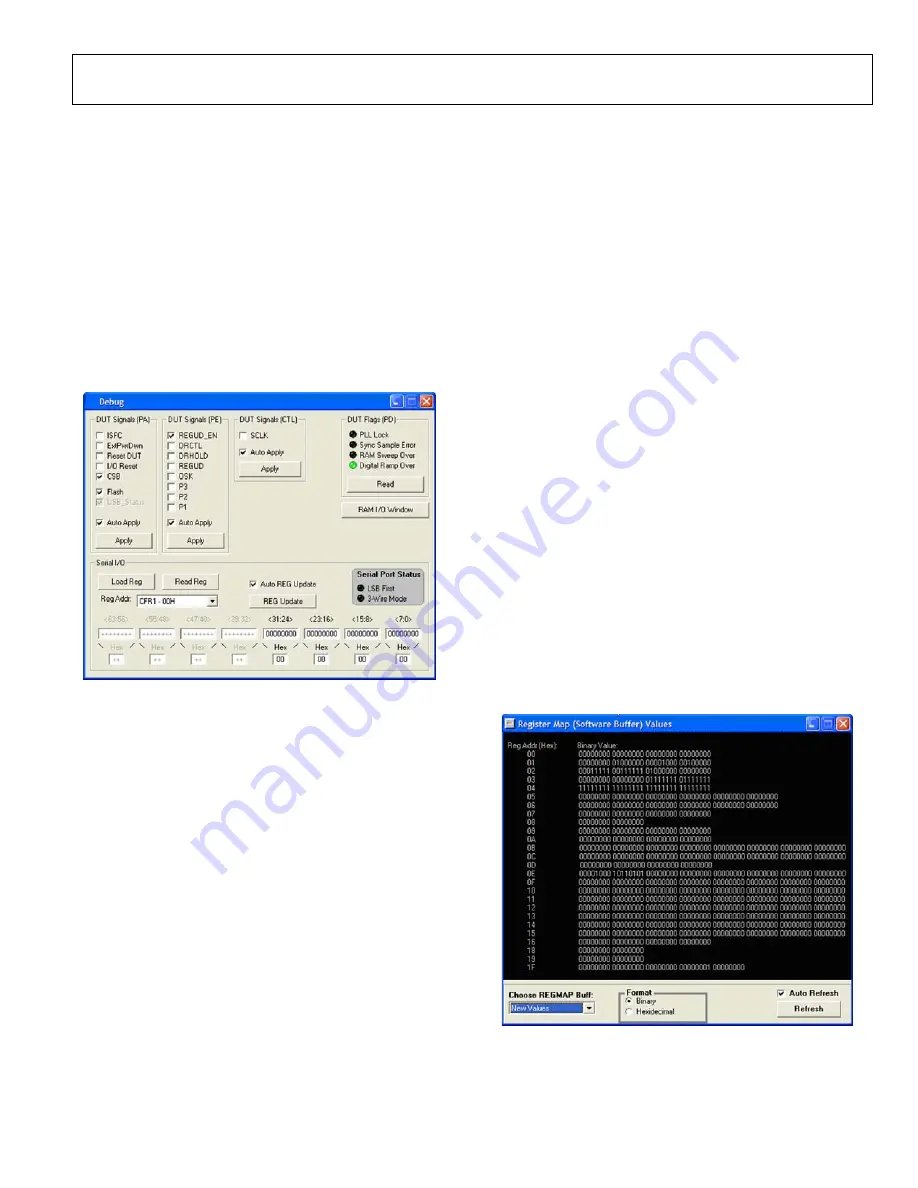
REGISTER MAP (SOFTWARE BUFFER) VALUES 

To access the 

Register Map (Software Buffer) Values

 window, 

select 

Register Map Values

 from the 

View 

drop-down menu (see 

Figure 10). 

07

48

1-

01

4


Figure 16. Register Map (Software Buffer) Values Window 

The 

Register Map (Software Buffer) Values 

window allows 

you to switch between the current values and the values that are 
loaded in the software buffer. This window does not allow 

Содержание AD9910

Страница 1: ...Factory tested and ready to use PACKAGE CONTENTS AD9910 evaluation board AD9910 PCBZ installation software CD USB cable GENERAL DESCRIPTION This user guide describes how to set up and use the AD9910 evaluation board The AD9910 is a 1 GSPS DDS with a 14 bit DAC The evaluation board software provides a graphical user interface GUI for easy communication with the device along with many user friendly ...

Страница 2: ... Driver 5 Launching the Program 5 Control Window 7 Profiles Window 9 Single Tone Mode 9 View Windows 11 OSK and Digital Ramp Control 12 Multichip Sync Control 13 RAM Operation 14 Debug 15 Register Map Software Buffer Values 15 REVISION HISTORY 10 10 Rev 0 to Rev A Document Title Changed from AD9910 PCBZ to UG 207 Universal Updated Format Universal Changes to Device Clock Oscillator Options Section...

Страница 3: ...k multiplier and connects through J1 The third option allows the user to connect a crystal resonator on the backside of the board Note that the AD9910 evaluation board does not populate the PLL loop filter components Therefore to use the internal PLL of the AD9910 the user must solder down these components or else the PLL is not stable The AD9910 data sheet has helpful formulas to calculate the ap...

Страница 4: ... multidevice synchronous operation DAC Output These connections represent the filtered or unfiltered default output of the DAC Clock Mode Select This connection controls whether the reference clock source is a 20 MHz to 30 MHz crystal or is from an external signal generator A 25 MHz crystal is provided on the underside of the AD9910 evaluation board Ref Clock Input This is the input for the extern...

Страница 5: ...ard After the window has disappeared the USB Status LED CR2 on the AD9910 evaluation board flashes which indicates that the evaluation board is connected properly Windows XP Users 1 Power up the AD9910 evaluation board see Table 2 2 Connect the evaluation board to the computer via the USB port using a USB cable Then the VBUS LED CR1 on the AD9910 evaluation board illuminates 3 When the USB cable i...

Страница 6: ... to scroll up and view the details and possible cause of the error see Figure 3 Most status message errors can be resolved by checking jumper settings making sure that the evaluation board is powered up correctly and inspecting the USB port and cable connections When all power USB port cable connections and jumper settings are correct an error may still appear if the clock input is not properly co...

Страница 7: ... selects the charge pump current output of the PLL in the reference clock multiplier circuitry Selecting a higher current output results in the loop locking faster but there is a trade off Increasing this current output also increases phase noise The default setting of this drop down box is 387 μA VCO Range allows you to select the range of operation for the VCO on the AD9910 The AD9910 evaluation...

Страница 8: ... current of the DAC This number is based on a DAC_RSET resistor value of 10 kΩ Setting Other Control Window Options Enable I O Sync Clock Output Pin allows you to enable or disable the output driver for the I O sync clock output Enable Matched Latency allows you to align the application of the frequency tuning word the phase offset word and the amplitude scale factor at the same time If this bit i...

Страница 9: ... has 14 bits of resolution Note that this can be used in conjunction with DAC Gain Ctrl in the AUX DAC Control section see Figure 5 to increase the flexibility of the output amplitude The spin boxes for amplitude SF are set to 1 bit by default The number of bits can be changed to your preference by typing in the spin box Data Entry Windows The Edit output frequency dialog box see Figure 7 appears ...

Страница 10: ...exadecimal or binary format This window also allows you to type in a tuning word and see the correct decimal hexadecimal or binary representation for this word The Output Scale Factor spin box allows you to scroll through the different tuning words one bit at a time using the up and down arrows 07481 008 Figure 9 Edit Output Scale Factor Pop Up Dialog Box Activate In the Activate area of the Profi...

Страница 11: ...ion Board User Guide UG 207 Rev A Page 11 of 16 VIEW WINDOWS To access additional windows select View from the AD9910 Evaluation Software drop down menu bar 07481 017 Figure 10 Windows Accessed from View Menu ...

Страница 12: ...te box allows you to reload the digital ramp rate when an I O update is issued or when there is a profile change Sweep Frequency 0 and Sweep Frequency 1 are the starting and stopping frequencies of the ramp Note that this is frequency phase or amplitude depending on which ramp generator is selected It is important that the value in the Sweep 0 register is always less than the value in the Sweep 1 ...

Страница 13: ...7481 010 Figure 12 Multi Chip Sync Window The Multi Chip Sync window allows you to set up the sync function This allows you to sync multiple chips to one master AD9910 Refer to the AD9910 data sheet for a full description on multichip sync functions The Input Sync Pulse Delay drop down box sets the input delay of the synchronization receiver in 150 ps steps The Output Sync Pulse Delay sets the out...

Страница 14: ... 16 bit address step rate value The Mode Control drop down box sets the 3 bit RAM control word mode See the AD9910 data sheet for a complete description of the RAM operating modes The Zero Crossing check box sets the zero crossing bit This bit is effective only in RAM mode using direct switch The No Dwell check box sets the no dwell high bit This bit is only effective when the RAM mode is in ramp ...

Страница 15: ...TL DRHOLD REGUD OSK P3 P2 and P1 check boxes control their selected pins REGUD issues an I O update to the device under test DUT whereas REGUD_EN allows the software to control the I O_UPDATE pin P3 P2 and P1 control the profile register pins See the AD9910 data sheet for the logic to control the profiles via the external pins DUT Signals CTL The SCLK serial clock pin check box is used to synchron...

Страница 16: ...sublicense or distribute the Evaluation Board and ii permit any Third Party to access the Evaluation Board As used herein the term Third Party includes any entity other than ADI Customer their employees affiliates and in house consultants The Evaluation Board is NOT sold to Customer all rights not expressly granted herein including ownership of the Evaluation Board are reserved by ADI CONFIDENTIAL...

Страница 17: ...Mouser Electronics Authorized Distributor Click to View Pricing Inventory Delivery Lifecycle Information Analog Devices Inc AD9910 PCBZ ...

Отзывы: