background image

AD9779 

Preliminary Technical Data


Rev. PrD | Page 22 of 34 

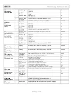
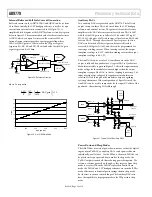
Internal Reference/Full Scale Current Generation


Full scale current on the AD9779 IDAC and QDAC can be set from 
10 to 30ma. Initially, the 1.2V bandgap reference is used to set up a 
current in an external resistor connected to I120 (pin 75). A 
simplified block diagram of the AD9779 reference circuitry is given 
below in 

Figure 29

. The recommended value for the external resistor 

is 10K 

, which sets up an I 

REFERENCE

 in the resistor of 120

µ

a.  

Internal current mirrors provide a current gain scaling, where 
IDAC or QDAC gain is a 10 bit word in the SPI port register 
(registers  0A, 0B,  0E, and 0F). The default value for the DAC gain 
registers gives an I

FS

 of 20ma. 


1.2V bandgap

10K

0.1

µ

F

current scaling

DAC full scale

reference current

IDAC

QDAC

AD9779

IDAC gain

QDAC gain

I120

VREF


Figure 29 . Reference Circuitry


where I

FS

 is equal to; 


32

gain


DAC

1024

6

12

27

R

1.2V

×

⎟⎟

⎜⎜

×

+

×


0

5

10

15

20

25

30

35

0

200

400

600

800

1000

DAC gain code

I

FS

 (m

a

)


Figure 30. I

FS

 vs. DAC Gain Code


Auxiliary DACs


Two auxiliary DACs are provided on the AD9779. The full scale 
output current on these DACs is derived from the 1.2V bandgap 
reference and external resistor. The gain scale from the reference 
amplifier to the DAC reference current for each aux DAC is 16.67.  
with the Aux DAC gain set to full scale (10 bit values, SPI reg 0C, 
0D, 10, 11), this gives a full scale current of 2ma for Aux DAC1 and 
for Aux DAC2.  Through these same SPI port registers, the Aux 
DACs can be turned off, their signs can be inverted (scale is 
reversed, 0-1024 gives I

FS

 to 0), and they can be programmed for 

sourcing or sinking current. When sourcing current, the output 
compliance voltage is 0-1.5V, and when sinking current the output 
compliance voltage is 0.8-1.5V. 
 
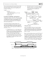
The Aux DACs can be used for LO cancellation when the DAC 
output is followed by a quadrature.  A typical DAC to Quadrature 
Modulator interface is given in Figure 31. Often, the input common 
mode voltage for the modulator is much higher than the output 
compliance range of the DAC, so that ac coupling is necessary. The 
input referred offset voltage of thee quadrature modulator can 
result in LO feed through on the modulator output, degrading 
system, performance. If the configuration of  

Figure 29

 is used, the 

Aux DACs can be used to compensate for the input DC offset of the 
quad mod,  thus reducing LO feedthrough.  
 

IOUT1_P

IDAC

QDAC

IOUT2_N

IOUT2_P

IOUT1_N

AUX1_P

AUX

DAC1

AUX2_N

AUX2_P

AUX1_N

AUX

DAC2

Quad Mod

I Inputs

Quad Mod

Q Inputs


Figure 31. Typical Use of Auxiliary DACs  


Power Down and Sleep Modes 

The AD9779 has a variety of power down modes, so that the digital 
engine, main TxDACs, or auxiliary DACs can be powered down 
individually, or all at once.  Via the SPI port, the main TxDACs can 
be placed in sleep or powered down modes. In sleep mode, the 
TxDAC output is turned off, thus reducing power dissipation. The 
reference remains powered on though, so that recovery from sleep 
mode is very fast. When the TxDAC is placed in Power Down 
mode, the TxDAC and 1.2V bandgap reference are turned off. This 
mode offers more substantial power savings than in sleep mode, 
but the time to turn on is much longer. The Auxiliary DACs also 
have the capability to be programmed via the SPI port into sleep 
mode.  

Содержание AD9779

Страница 1: ...frequency It includes features optimized for direct conversion transmit applications including complex digital modulation and gain and offset compensation The DAC outputs are optimized to interface se...

Страница 2: ...ers 13 Notes on Serial Port Operation 13 SPI Register Map 14 Internal Reference Full Scale Current Generation 22 Auxiliary DACs 22 Power Down and Sleep Modes 22 Internal PLL Clock Multiplier Clock Dis...

Страница 3: ...Reference TBD FSR Full Scale Output Current 10 20 30 mA Output Compliance Range 1 0 V Output Resistance TBD k ANALOG OUTPUTS Output Capacitance TBD pF Offset TBD ppm C Gain TBD ppm C TEMPERATURE DRIF...

Страница 4: ...tput Noise IoutFS 20mA TBD pA rtHz fDAC 100 MSPS fOUT 20 MHz 82 dBc fDAC 200 MSPS fOUT 50 MHz 82 dBc fDAC 400 MSPS fOUT 70 MHz 84 dBc SPURIOUS FREE DYNAMIC RANGE SFDR fDAC 800 MSPS fOUT 70 MHz 87 dBc...

Страница 5: ...4 VREF Voltage Reference Output 25 P1D 9 Port 1 Data Input D9 75 I120 120 A Reference Current 26 P1D 8 Port 1 Data Input D8 76 VDDA33 3 3 V Analog Supply 27 P1D 7 Port 1 Data Input D7 77 VSSA Analog C...

Страница 6: ...1D 0 P1D 1 P1D 2 P1D 3 VDDD18 VSSD P1D 4 P1D 5 P1D 6 P1D 7 P1D 8 P1D 9 27 26 P2D 7 P2D 8 P2D 9 P2D 10 50 49 AUX1_P VSSA VDDA33 VSSA VDDA33 CLK CLK VDDC18 VSSC VSSC 3 2 VDDC18 VSSC VSSC VDDC18 1 VDDC18...

Страница 7: ...H 35 2315 H 22 H 34 0 H 23 H 33 3671 H 24 H 32 0 H 25 H 31 6642 H 26 H 30 0 H 27 H 29 20755 H 28 32768 Table 6 Halfband Filter 2 Lower Coefficient Upper Coefficient Integer Value H 1 H 23 2 H 2 H 22 0...

Страница 8: ...Response to 4x Input Data Rate Dotted Lines Indicate 1dBRoll Off 4 3 2 1 0 1 2 3 4 100 90 80 70 60 50 40 30 20 10 0 10 Figure 4 AD9779 4x Interpolation Low Pass Response to 4x Input Data Rate Dotted...

Страница 9: ...ut MHz SFDR dBm FDATA 100MSPS FDATA 160MSPS FDATA 200MSPS Figure 8 SFDR vs FOUT 1x Interpolation 50 55 60 65 70 75 80 85 90 95 100 0 20 40 60 80 100 Fout MHz SFDR dBm FDATA 100MSPS FDATA 160MSPS FDATA...

Страница 10: ...FDATA 125MSPS FDATA 150MSPS FDATA 200MSPS Figure 14 Third Order IMD vs FOUT 4x Interpolation 50 60 70 80 90 100 0 50 100 150 200 250 300 350 400 450 Fout MHz IMD dBc 50MSPS 100MSPS FDATA 62 5MSPS 112...

Страница 11: ...3 0 4 0 5 0 6 0 7 0 25 50 75 100 125 150 175 200 225 250 FDATA MSPS Power W 8x Interpolation Zero Stuffing 4x Interpolation Zero Stuffing 4x Interpolation 2x Interpolation Zero Stuffing 2x Interpolat...

Страница 12: ...ow will reset the SPI port timing to the initial state of the instruction cycle This is true regardless of the present state of the internal registers or the other signal levels present at the inputs...

Страница 13: ...rator increments for each byte of the multibyte communication cycle The AD9779 serial port controller data address will decrement from the data address written toward 0x00 for multibyte I O operations...

Страница 14: ...e Sync Driver Enable Dac Clock Offset 2 0 00h Interrupt Register 06h 06 Data Delay IRQ Sync Delay IRQ Cross Control IRQ Data Delay IRQ Enable Sync Delay IRQ Enable Cross Control IRQ Enable 00h 07h 07...

Страница 15: ...Delay 3 0 00h Cross Register 15h 20 Cross Run Cross Status Cross Done Cross Wiggle 2 0 Cross Step 1 0 00h Analog Write 16h 23 Analog Write 7 0 00h 17h 21 Mirror Roll Off 1 0 Band Gap Trim 2 0 00h Anal...

Страница 16: ...Enable Q path for signal processing 1 Disable Q path data clocks disabled 0 3 Inverse Sinc Enable 0 Inverse sinc disabled 1 Inverse sinc disabled 0 2 DATACLK Invert 0 Output DATACLK same phase as inte...

Страница 17: ...lter Bandwidth Tuning Recommended Settings See Table 14 for PLL Band Select values 000 PLL band select 00000 00111 100 PLL band select 01000 01111 110 PLL band select 10000 10111 111 PLL band select 1...

Страница 18: ...0000 13 Cross Point Upper Delay 7 0 Dndelay Value below zero for lower cross delay bits 7 6 unused 00000000 7 3 Cross Control Clock Delay Divide rate of CNTCLK by 2 3 0 CNTCLK 1 16 DAC clock rate 0000...

Страница 19: ...or off 1 Internal data generator on 0 1A MISR Control 2 0 Test Mode 000 Normal data port operation 001 111 To be defined test modes 000 1B MISR Signature Register 1 7 0 MISR Signature 31 24 Slice of 3...

Страница 20: ...125 8 0Ah 2 2 5 3F 8_even 6 0 575 0 625 0 675 8 0Bh 3 3 6 3F 8_odd 5 0 6375 0 6875 0 7375 8 0Ch 0 4 6 2F 8_even 4 0 7 0 75 0 8 8 0Dh 1 5 6 2F 8_odd 3 0 7625 0 8125 0 8625 8 0Eh 2 6 7 F 8_even 2 0 825...

Страница 21: ...0110 22 1032 1089 10101 21 1060 1119 10100 20 1089 1149 10011 19 1118 1179 10010 18 1148 1210 10001 17 1176 1239 10000 16 1206 1270 01111 15 1237 1302 01110 14 1268 1334 01101 13 1299 1366 01100 12 13...

Страница 22: ...d scale is reversed 0 1024 gives IFS to 0 and they can be programmed for sourcing or sinking current When sourcing current the output compliance voltage is 0 1 5V and when sinking current the output c...

Страница 23: ...he ratio of Reference Clock Input Data Rate The VCO runs optimally over the range 804MHz to 1800MHz so that N1 is used to keep the speed of the VCO in this range even though the DAC sample rate may be...

Страница 24: ...es of up to 250MSPS the AD9779 has a fine timing feature Fine timing adjustments can be made by programming values into the DATA CLOCK DELAY register reg 03h 5 3 By changing the values in this registe...

Страница 25: ...1 4 3 2 2 3 4 1 1 2 3 4 1 2 5 7 8 6 3 4 5 6 7 8 Figure 39 Nyquist Zones Figure 3 Figure 4 and Figure 5 show the low pass response of the digital filters with no modulation used By turning on the modu...

Страница 26: ...ass band will now be centered at 3 5 FDATA However the signal will still remain at the same place in the spectrum The even odd mode capability allows the passband to be placed anywhere in the DAC Nyqu...

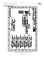
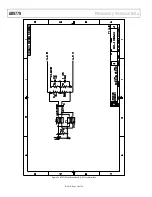
Страница 27: ...Preliminary Technical Data AD9779 Rev PrD Page 27 of 34 EVALUATION BOARD SCHEMATICS Figure 47 AD9779 Eval Board Rev B Power Supply Decoupling and SPI Interface...

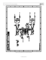
Страница 28: ...AD9779 Preliminary Technical Data Rev PrD Page 28 of 34 Figure 48 AD9779 Eval Board Rev B Circuitry Local to AD9779...

Страница 29: ...Preliminary Technical Data AD9779 Rev PrD Page 29 of 34 Figure 49 AD9779 Eval Board RevB AD8349 Quadrature Modulator...

Страница 30: ...AD9779 Preliminary Technical Data Rev PrD Page 30 of 34 Figure 50 AD9779 Eval Board RevB DAC Clock Interface...

Страница 31: ...Preliminary Technical Data AD9779 Rev PrD Page 31 of 34 Figure 51 AD9779 Eval Board RevB Input Port 1 Digital Input Buffers...

Страница 32: ...AD9779 Preliminary Technical Data Rev PrD Page 32 of 34 Figure 52 AD9779 Eval Board RevB Input Port 2 Digital Input Buffers...

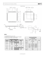
Страница 33: ...Preliminary Technical Data AD9779 Rev PrD Page 33 of 34 Outline Dimensions...

Страница 34: ...proprietary ESD protection circuitry permanent damage may occur on devices subjected to high energy electrostatic discharges Therefore proper ESD precautions are recommended to avoid performance degr...

Отзывы: