background image

UG-002 

Evaluation Board User Guide


Rev. 0 | Page 10 of 12 

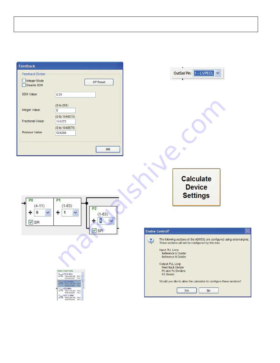
Feedback Window 

Clicking 

Click for Details

 in the 

Feedback Divider

 box of the 

main window accesses the 

Feedback 

window, which allows you 

to change the feedback divider settings (see Figure 15). 

08129-

017


Figure 15. Feedback Window 

P0, P1, and P2 (Output Dividers) Boxes 

Selecting the 

SPI

 check box in any of the divider settings boxes 

(that is, the P0, P1, or P2 box) in the main window enables a 
drop-down selection of predetermined divider settings (see 
Figure 16). 

08

12

9-

0

18


Figure 16. P0, P1, and P2 Boxes (in Main Window) 

Output Loop Config: Box 

The 

Output Loop Config:

 box can be used to change the output 

frequency of the AD9551. This control changes the logic levels 
of the output frequency selection pins of the AD9551. 

08

12

9-

02

9


Figure 17. Output Loop Config: Box (in Main Window) 

OutSel Pin: Box 

The 

OutSel Pin:

 drop-down box (see Figure 18) in the main 

window controls the logic level on the OUTSEL pin of the 
AD9551. However, this value can be overwritten by using the 
SPI control register. 

08

12

9-

01

9


Figure 18. OutSel Pin Box (in Main Window) 

USING SOFTWARE TO CALCULATE THE DEVICE 
SETTINGS 

The following procedure explains how the evaluation board 
software can be used to automatically calculate and set the 
settings to program the AD9551.  

In this example, the input frequency is 122.88 MHz on REF A, 
and the output frequency is 122.88 MHz. 

1.


Ensure that Jumper JMP3 is positioned for PC control. 

2.


Verify that all five jumpers are in place on Connector P2. 

3.


Set the positions of the S1, S2, and S3 dip switches to high. 

4.


Click 

Calculate Device Settings

 in the main window of the 

evaluation board software.  

08

12

9-

0

20


Figure 19. Calculate Device Settings Button (in Main Window) 

5.


The 

Enable Control?

 window, shown in Figure 20, 

appears.  

08

129-

021


Figure 20. AD9551 Serial Port Programming Warning 

6.


Click 

Yes

 to enable serial port register programming. 

Содержание AD9551

Страница 1: ...AD9551 evaluation board and includes detailed schematics and PCB layout artwork The AD9551 Revision D evaluation board is a compact easy to use platform for evaluating all features of the AD9551 multi...

Страница 2: ...d Software 4 Installing the Software 4 Using the Software 4 Guide to Programming the AD9551 5 Using an SPI Port 5 Using Dip Switches Manual Control 5 Using Software to Override Dip Switches Software C...

Страница 3: ...Next The Found New Hardware Wizard may appear twice and a system restart may be required Refer to the Evaluation Board Software section for details on running the AD9551 evaluation board software SET...

Страница 4: ...the evaluation board to the PC 2 Double click AD9551 Eval Software to run the AD9551 evaluation software A hardware installation window appears Depending on whether the evaluation board was found by...

Страница 5: ...s to low Note that S2 controls REF B If REF B is not used there is no need to change the S2 settings 4 Connect a signal generator to REF A SMA Connector J1 By default the reference inputs on this eval...

Страница 6: ...re outlined in this section From the main window the window for each functional block can be accessed by clicking the appropriate box in the main window When a subsection window closes after clicking...

Страница 7: ...u allows you to select which evaluation board the software controls see Figure 5 Click Refresh List to detect a recently connected evaluation board 08129 005 Figure 5 Select USB Device Window Selectin...

Страница 8: ...ion boxes in the main window have a checkbox labeled SPI If this box is selected the software allows serial port writes when conditions are changed in the corresponding subsection window When a subsec...

Страница 9: ...Input PLL DCXO Window Clicking Click for Details in the PLL DCXO box in the main window accesses the Input PLL DCXO window see Figure 12 08129 014 Figure 12 Input PLL DCXO Window PFD and Charge Pump W...

Страница 10: ...e OutSel Pin drop down box see Figure 18 in the main window controls the logic level on the OUTSEL pin of the AD9551 However this value can be overwritten by using the SPI control register 08129 019 F...

Страница 11: ...ioned for PC control 2 Verify that all five jumpers are in place on Connector P2 3 Set the positions of the S1 S2 and S3 dip switches to high 4 Click Calculate Device Settings in the main window of th...

Страница 12: ...ings that have not been loaded to the AD9551 evaluation board Click LOAD to load these settings to the evaluation board 4 Select 19 44MHz Mode in the Input PLL Mode box and then click OK ESD CAUTION 5...

Отзывы: